

Welcome to Renesas' PCI Express® Timing blog where we will discuss all things related to PCIe timing, including specifications, clocking architectures, measurement techniques and, of course, timing devices.
First, a snapshot of where we are. The PCI SIG ratified version 1.0 of the PCIe Gen4 specification in September 2017. The PCIe Gen5 specification moved to version 0.7 at the end of April 2018 and is targeting a version 0.9 release in September 2018. Things are moving much more quickly for the Gen5 specification than they did for Gen4. Today most new design activity centers on PCIe Gen3 or Gen4 and it is premature to delve into PCIe Gen5 designs, so we’ll keep our focus on PCIe Gen3 and Gen4 for now.
Before we dive in, I would like to note that a beneficial characteristic of PCIe Gen4 is that the calculations for clock jitter are the same as for Gen3. The only difference is that the PCIe Gen4 jitter limit is 500fs rms, instead of the 1ps rms for Gen3. This means that if you calculate your clock jitter using the PCIe Gen3 calculations and your result is less than 500fs rms, you can use the clock for PCIe Gen4.
Phase noise measurement techniques for PCI Express clocks differ significantly from those used for networking clocks. The remainder of this blog post compares and contrasts the two.
Let’s start with the popular 12kHz – 20MHz brick wall filter often used with phase noise analyzers (PNAs) to measure network clocks, see Figure 1. The linear vertical scale is in dBc/Hz (decibels with respect to the carrier at each frequency) and the log horizontal scale is in Hz. For PCIe timing, the carrier is the 100MHz clock. Ethernet clocking often uses 156.25MHz.
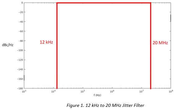
A brief inspection reveals that there is no attenuation in the “pass band” between 12kHz and 20MHz, shown by the horizontal line at 0dBc. The vertical lines at 12kHz and 20MHz completely attenuate the frequencies outside the pass band. We refer to these vertical lines as a “brick wall” filter. This means that the jitter calculation includes all noise in the pass band region and excludes all noise outside the pass band. This filter is equally sensitive to all noise content in the pass band.
Figure 2 illustrates the filter combinations applied to the PCIe clock jitter before calculating the jitter. PCIe Gen3 and Gen4 clock jitter is the worst value obtained after applying the 64 filter combinations. This worst value must be less than the specification limit.
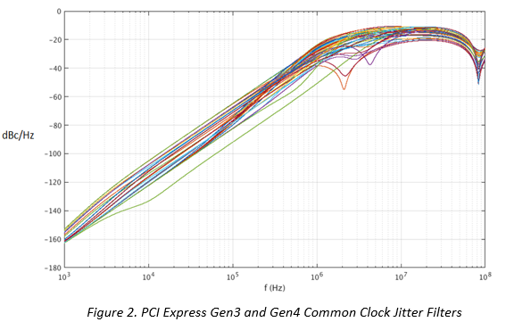
Inspecting Figure 2 shows significant differences from the 12kHz – 20MHz filter of Figure 1. The most obvious difference is that there is no brick wall. Instead, there is 20dB/decade of attenuation below 1MHz. (Note: A decade is a power of 10 on the log scale [104 to 105, 105 to 106]). This attenuation works for common clocked systems because we assume low frequency noise is common and we specify all PLL’s (clock PLLs and TX/RX PLLs) to track it. This implies that PCIe Gen3 and Gen4 Common Clock systems are less sensitive to low frequency clock jitter than networking systems. This is also why very good PCIe clocks for common clocked systems often have relatively high 12kHz – 20MHz phase jitter numbers. This is also why clocks specified for common clock systems cannot necessarily be used in separate clock systems. (We will cover this topic in a future post).
The next item to note is that the filters pass most noise above 1MHz, in fact, the filters are fairly flat above 1MHz. This implies that PCIe Gen3 and Gen4 common clock timing is most sensitive to jitter above 1MHz.
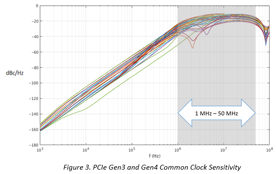
Another significant difference between PCIe and networking clock jitter measurements is not evident from Figure 2. Digital sampling oscilloscopes (DSOs) are used to obtain clock period or waveform files to calculate PCIe clock jitter, rather than PNAs. The main reason for this is that PCIe clocking supports spread spectrum while network clocking does not and, historically, PNAs have been unable to work with a clock that is spreading.
From Nyquist, the act of sampling a signal aliases all information down to f/2. For a 100MHz PCIe clock this means that the file obtained from the DSO contains useful information up to 50MHz. This also means that PCIe clock jitter calculations based on data from DSOs calculate all the way up to 50MHz! Even though the filters are at approximately -20dBc above 1MHz, PCIe Gen3 and Gen4 common clock jitter is most sensitive in a range from 1MHz all the way to 50MHz as shown in Figure 3.
Thanks for reading and stay tuned for further PCIe clocking insights. Visit renesas.com/pcietiming for more information, including the latest products, evaluation tools and videos.