
Low Skew, 1-to-8 LVCMOS Clock Multiplier/Zero Delay Buffer
以下のデバイスを代替品として推奨しております。
ページセクションへ移動:
概要
説明
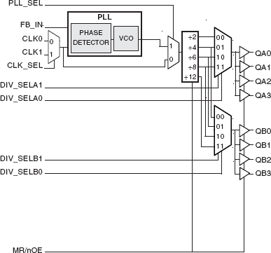
The 8752 is a low voltage, low skew LVCMOS clock generator. With output frequencies up to 240MHz, the 8752 is targeted for high performance clock applications. Along with a fully integrated PLL, the 8752 contains frequency configurable outputs and an external feedback input for regenerating clocks with "zero delay".
Dual clock inputs, CLK0 and CLK1, support redundant clock applications. The CLK_SEL input determines which reference clock is used. The output divider values of Bank A and B are controlled by the DIV_SELA0:1, and DIV_SELB0:1, respectively.
For test and system debug purposes, the PLL_SEL input allows the PLL to be bypassed. When HIGH, the MR/nOE input resets the internal dividers and forces the outputs to the high impedance state.
The low impedance LVCMOS outputs of the 8752 are designed to drive terminated transmission lines. The effective fanout of each output can be doubled by utilizing the ability of each output to drive two series terminated transmission lines.
特長
- Fully integrated PLL
- Eight LVCMOS outputs, 7Ω typical output impedance
- Selectable LVCMOS CLK0 or CLK1 inputs for redundant clock applications
- Input/Output frequency range: 18.33MHz to 240MHz at VCC = 3.3V ± 5%
- VCO range: 220MHz to 480MHz
- External feedback for "zero delay" clock regeneration
- Cycle-to-cycle jitter: 75ps (maximum), (all outputs are the same frequency)
- Output skew: 100ps (maximum)
- Bank skew: 55ps (maximum)
- Full 3.3V or 2.5V supply voltage
- 0°C to 70°C ambient operating temperature
- Available in lead-free RoHS-compliant package
製品比較
アプリケーション
設計・開発
モデル
ECADモデル
[製品選択]テーブル内の製品名をクリックするとSamacSysが提供する回路図シンボル、PCBフットプリント、3D CADモデルがご確認いただけます。 お探しのシンボルやモデルが見つからない場合、Webサイトから直接リクエストできます。

Processing table
| TQFP | 32 | C | Yes | Tray | ||
| TQFP | 32 | C | Yes | Reel |

Tips for Using This Parametric Table:
- Hide Filters button in header: Collapse or expands filters
- Column sort buttons in header: Sort Column alphabetically / numerically descending or ascending
- Reset button in header: Reset all filters to the page default
- Full Screen button in header: Expand the table to full screen view (user must close out of full screen before they can interact with rest of page)
- Export button in header: Export the filtered results of the table to an Excel document
- Filter parts search bar in header: Type to filter table results by part number
- Hide column button in column headers: Select to hide columns in table
- AND / OR toggle switches in header: Toggles the logic of this particular filter to be “AND” or “OR” logic for filtering results
- Multiselect checkboxes at beginning of each row in table: Select these checkboxes to compare products against each other
- Document icon next to product name in row: View the featured document for this product
- Chip icon next to the right of the document icon in row: View the block diagram for this product
- Cart icon to the right of the chip icon: Indicates that samples are available for this product