-
-
-
Design Resources
- Design & Development
- Featured Design Tools
- Partners
- Content & Training
-
Support
-
Support Forums
Get help from our expert Renesas technical staff and community.
- Technical Support
- Training & Events
- Quality & Packaging
-
Support Forums
-
Sample & Buy
-
Buy Direct from Renesas
Customers can now choose the convenience of buying direct from Renesas.
- Ordering Resources
-
Buy Direct from Renesas
CD4042BMS
circleLast Time BuySamples AvailableCMOS Quad D Latch, Clocked
Jump to Page Section:
arrow_drop_down
Overview
Description
The CD4042BMS radiation hardened Quad D latch contains four latch circuits, each strobed by a common clock. Complementary buffered outputs are available from each circuit. The impedance of the n- and p-channel output devices is balanced and all outputs are electrically identical.
Features
- High-Voltage Type (20V Rating)
- Clock Polarity Control
- Q and Q Outputs
- Common Clock
- Low Power TTL Compatible
- Standardized Symmetrical Output Characteristics
- 100% Tested for Quiescent Current at 20V
- Maximum Input Current of 1μA at 18V Over Full Package Temperature Range; 100nA at 18V and +25 °C
- 5V, 10V, and 15V Parametric Ratings
- Noise Margin (Over Full Package Temperature Range):
- 1V at VDD = 5V
- 2V at VDD = 10V
- 2.5V at VDD = 15V
- Meets All Requirements of JEDEC Tentative Standard No. 13B, "Standard Specifications for Description of 'B' Series CMOS Devices"
Comparison
Applications
Applications
- Buffer Storage
- Holding Register
- General Digital Logic
Documentation
Log in required to subscribe
|
|
|
|
|---|---|---|
| Type | Title | Date |
| Brochure | PDF 467 KB | |
| Brochure | PDF 4.85 MB | |
| Price Increase Notice | PDF 360 KB | |
| Other | ||
| White Paper | PDF 533 KB | |
| Product Advisory | PDF 499 KB | |
| Product Change Notice | PDF 230 KB | |
| Application Note | PDF 338 KB | |
| Application Note | PDF 224 KB | |
9 items
|
||
Design & Development
Models
ECAD Models
Schematic symbols, PCB footprints, and 3D CAD models from SamacSys can be found by clicking on products in the Product Options table. If a symbol or model isn't available, it can be requested directly from the website.

Product Options
Please log in or register to buy
Log in to order
Processing table
Pkg. Type |
Carrier Type |
MOQ |
DLA SMD |
Buy / Sample |
|
|---|---|---|---|---|---|
| Part Number | |||||
CD4042BDMSR circleLast Time Buy Samples Available |
SBDIP | Tube | 25 | 5962R9663301VEC | Get Samples, |
CD4042BKMSR circleLast Time Buy Samples Available |
CFP | Tray | 25 | 5962R9663301VXC | Get Samples, |

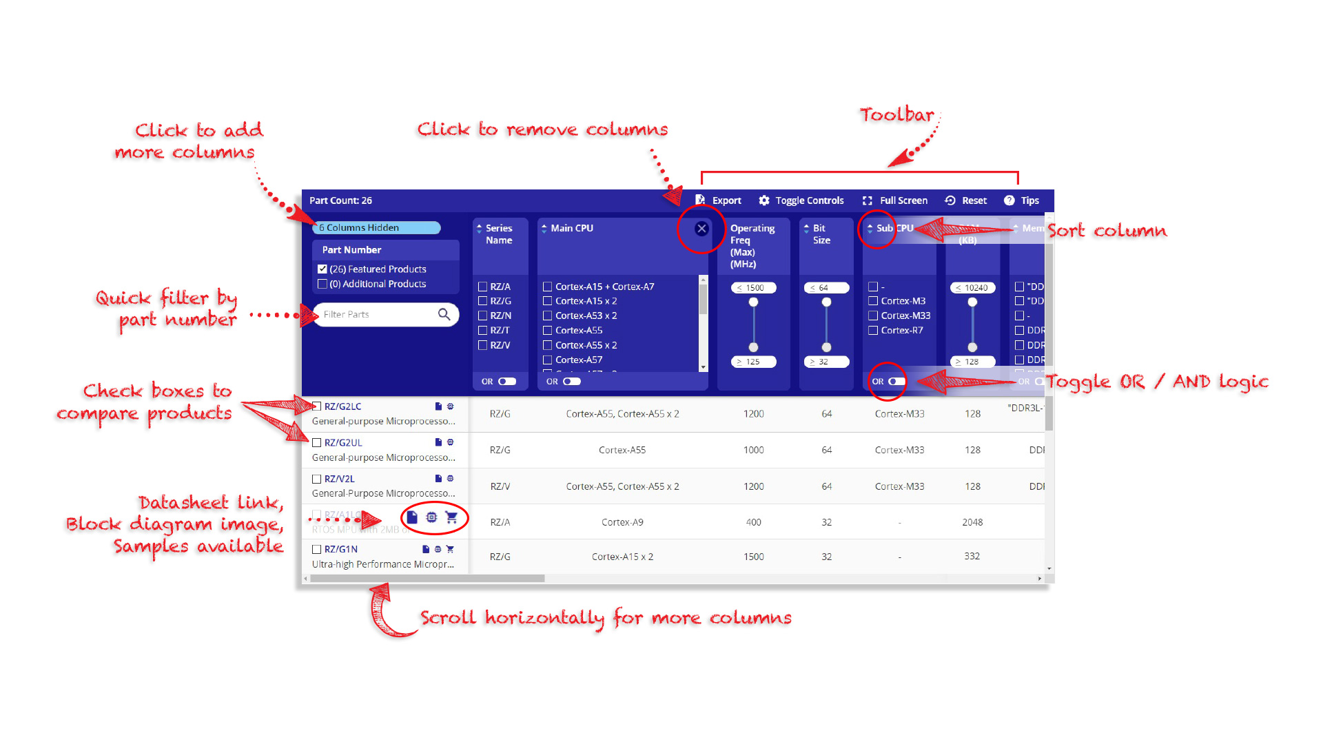
Tips for Using This Parametric Table:
- Hide Filters button in header: Collapse or expands filters
- Column sort buttons in header: Sort Column alphabetically / numerically descending or ascending
- Reset button in header: Reset all filters to the page default
- Full Screen button in header: Expand the table to full screen view (user must close out of full screen before they can interact with rest of page)
- Export button in header: Export the filtered results of the table to an Excel document
- Filter parts search bar in header: Type to filter table results by part number
- Hide column button in column headers: Select to hide columns in table
- AND / OR toggle switches in header: Toggles the logic of this particular filter to be “AND” or “OR” logic for filtering results
- Multiselect checkboxes at beginning of each row in table: Select these checkboxes to compare products against each other
- Document icon next to product name in row: View the featured document for this product
- Chip icon next to the right of the document icon in row: View the block diagram for this product
- Cart icon to the right of the chip icon: Indicates that samples are available for this product