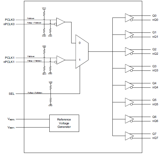
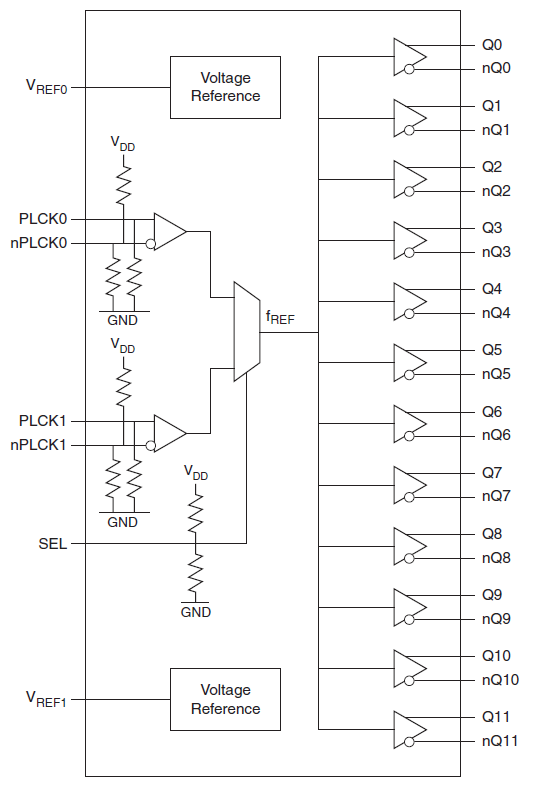
Image


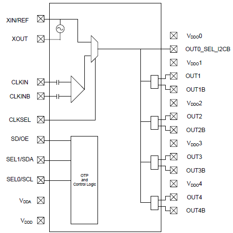
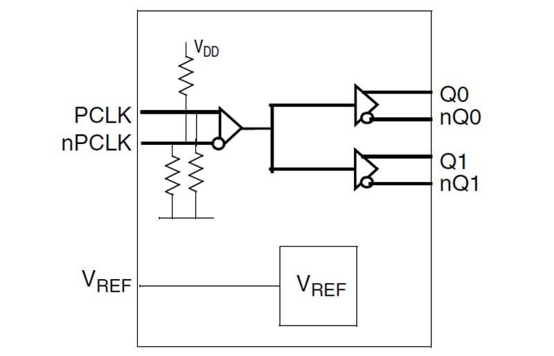
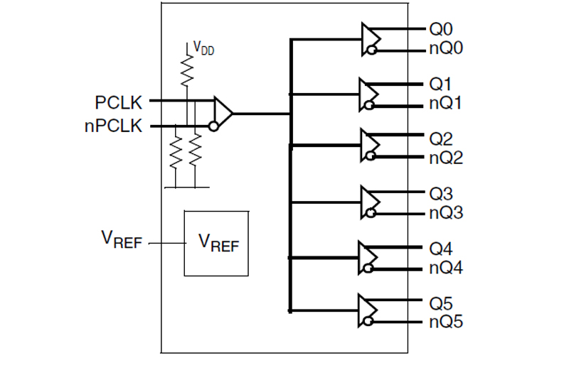
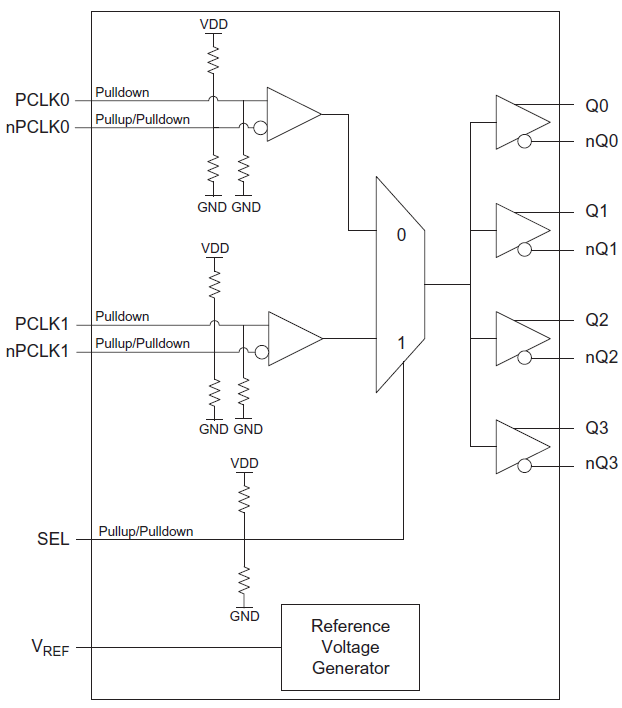
Renesas clock distribution products are used to condition, manipulate and distribute clock signals within a system, with or without the use of a phase-locked loop (PLL). These devices are well-suited for most applications where the input signal is of good quality, and the goal is to buffer, fan-out, divide or multiplex the input signal. A single-output clock buffer is also useful for translating a clock from one signaling standard to another, such as LVCMOS-in to LVPECL-out.
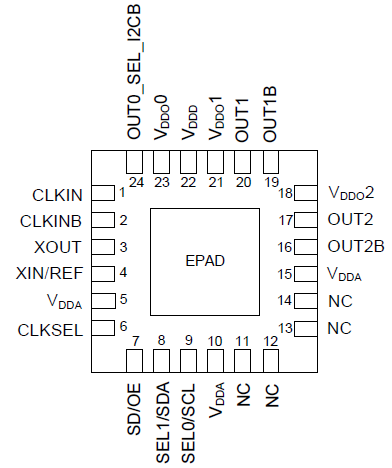
As the industry leader in timing solutions, Renesas offers a rich portfolio of clock buffer, clock distribution and multiplexer solutions to meet the needs of virtually any application. Renesas has the largest portfolio of clock distribution devices that support differential signals. LVDS, LVPECL, HCSL, LVCMOS, CML, HSTL, SSTL are some of the most common I/O levels supported by these devices.
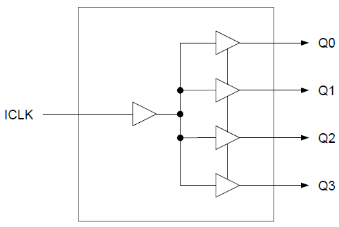
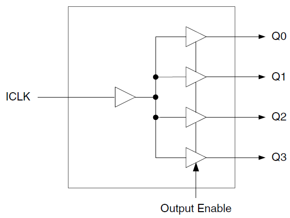
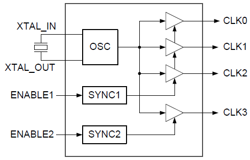
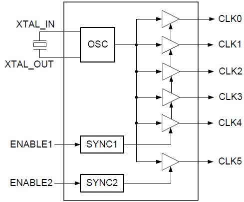
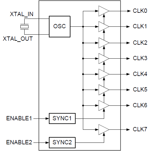
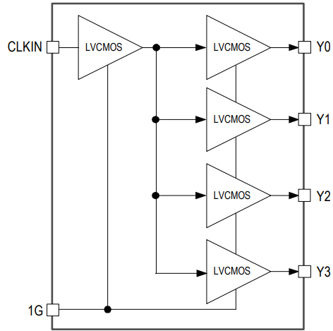
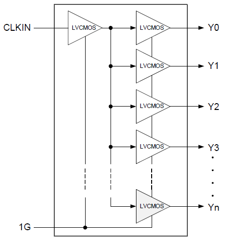
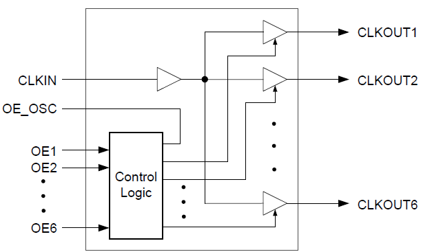
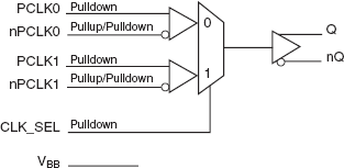
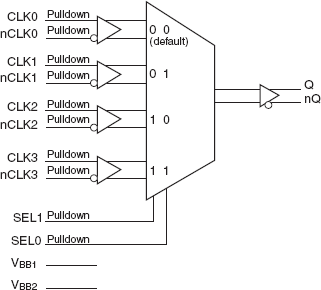
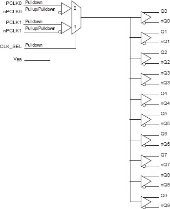
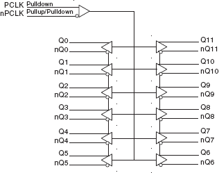
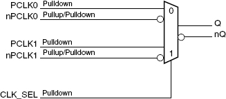
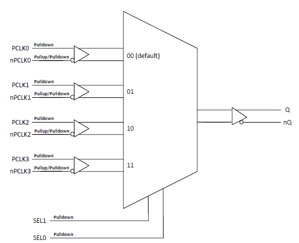
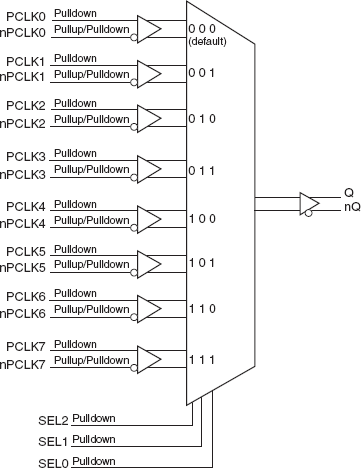
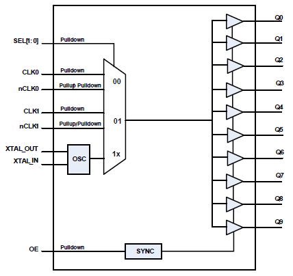
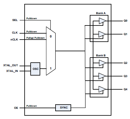
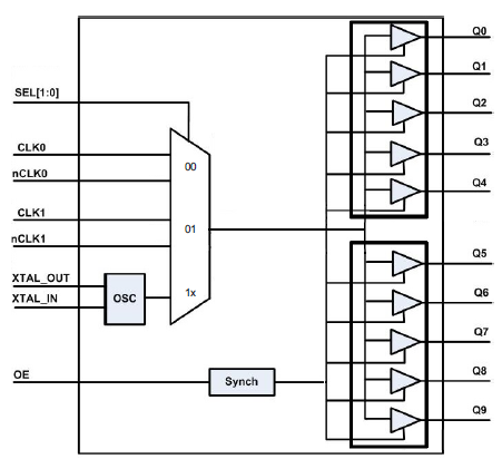
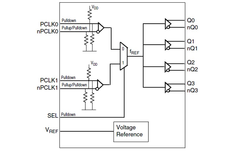
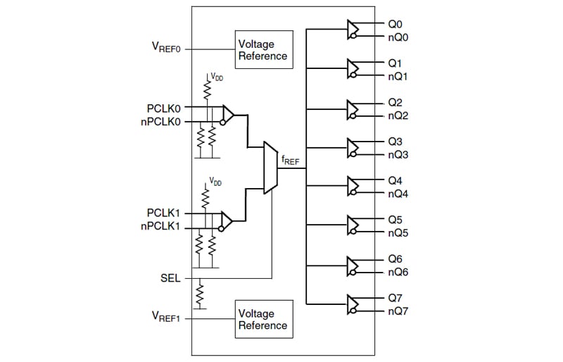
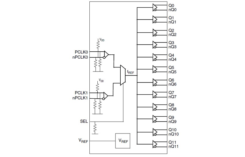
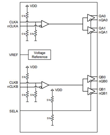
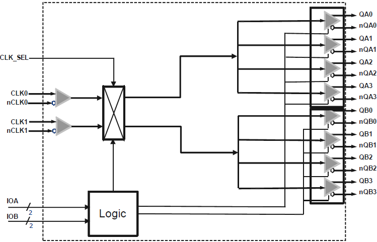
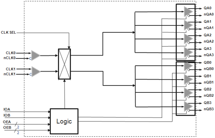
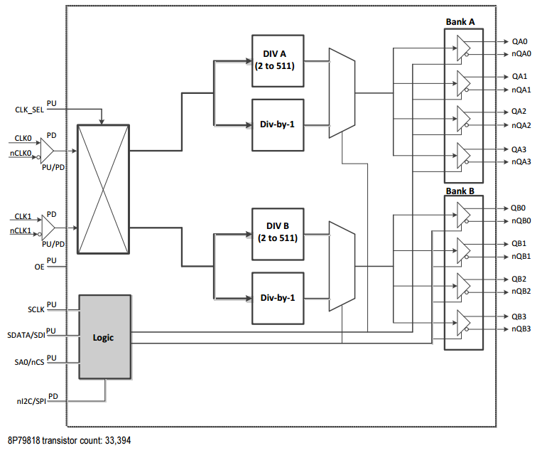
Clock distribution devices can be classified in many different ways. In some cases, a designer may want to take the incoming clock and distribute it out to multiple destinations without modifying the clock frequency. In other cases, the designers may need to divide it down or multiplex it with other clocks.
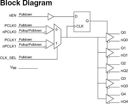
There are also clock distribution applications where a zero delay buffer may be needed. These are PLL-based devices that regenerate the input clock signal with fanout to drive multiple loads. Most devices allow the delay through the device to be adjusted through an external feedback path.
About the Clock Distribution Network
A clock distribution network (often referred to as a clock tree) distributes clock signals from a common source to all the electrical components that require it. This function is vital to the operation of a synchronous system, so much attention must be given to the characteristics of the clock signals and the electrical networks used in their distribution. The proper design of the clock distribution network helps ensure that critical timing requirements are satisfied, resulting in reliable operation and optimal performance.
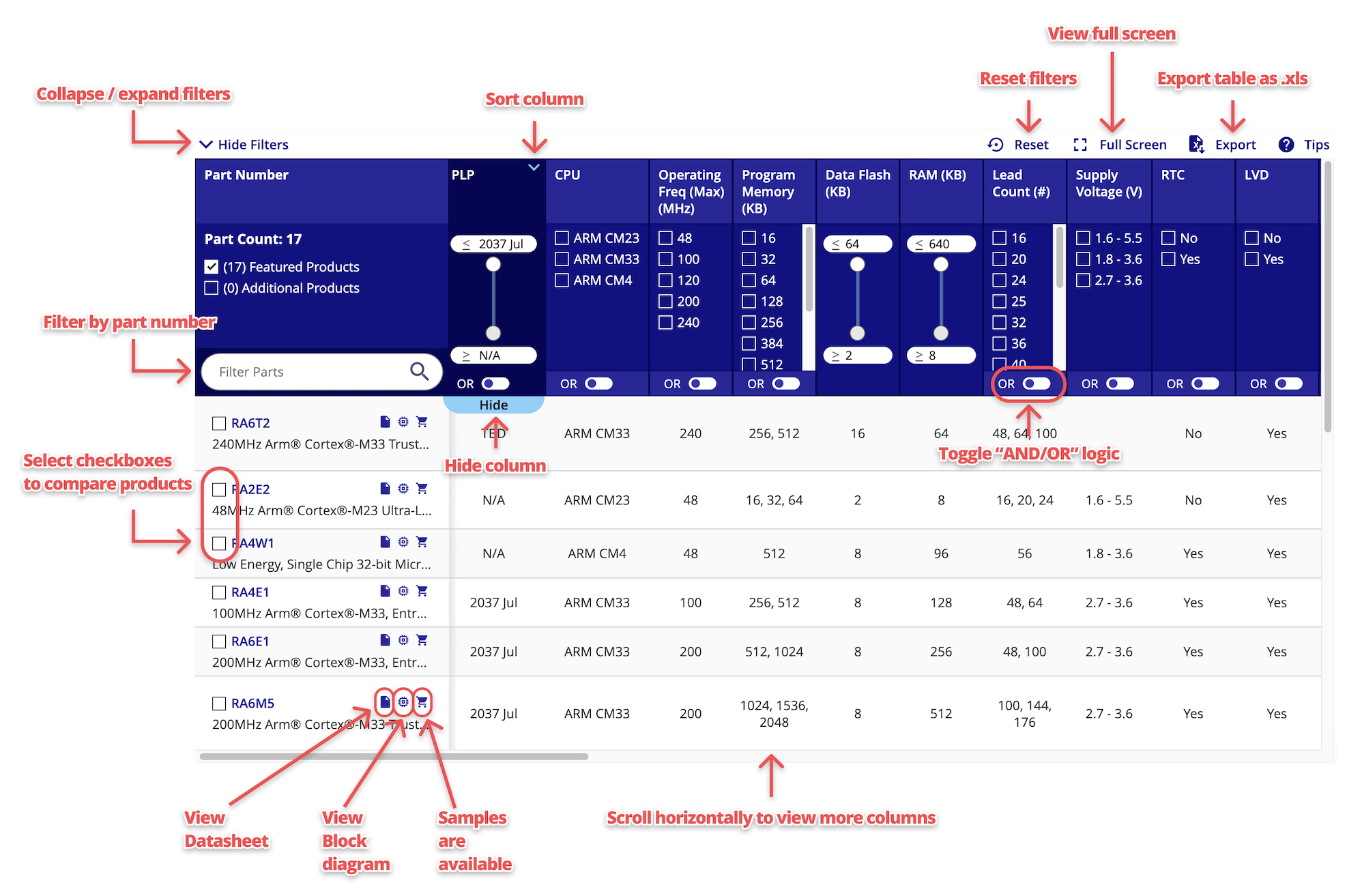
Subcategory |
Temp. Range |
Pkg. Type |
Lead Count (#) |
Pkg. Dimensions (mm) |
|
|---|---|---|---|---|---|
| Part Number | |||||
| Low Skew 1 to 4 Clock Buffer | Clock Buffers & Drivers | -40 to 85°C | COL, SOIC | 8 | 2.0 x 2.0 x 0.5, 4.9 x 3.9 x 1.5 |
| Low Skew 1 to 4 Clock Buffer | Clock Buffers & Drivers | -40 to 85°C | COL, SOIC | 8 | 2.0 x 2.0 x 0.5, 4.9 x 3.9 x 1.5 |
| Programmable Fanout Buffer | Clock Buffers & Drivers | -40 to 85°C | VFQFPN | 24 | 4.0 x 4.0 x 0.9 |
| Programmable Fanout Buffer | Clock Buffers & Drivers | -40 to 85°C | VFQFPN | 24 | 4.0 x 4.0 x 0.9 |
| 1.8 V to 3.3 V 1:4 Crystal Input to LVCMOS Output High-Performance Clock Fanout Buffer with OE | Clock Buffers & Drivers | -40 to 105°C | COL, TSSOP | 16 | 2.5 x 2.5 x 0.5, 5.0 x 4.4 x 1.0 |
| 1.8 V to 3.3 V 1:6 Crystal Input to LVCMOS Output High-Performance Clock Fanout Buffer with OE | Clock Buffers & Drivers | -40 to 105°C | COL, TSSOP | 16 | 2.5 x 2.5 x 0.5, 5.0 x 4.4 x 1.0 |
| 1.8 V to 3.3 V 1:8 Crystal Input to LVCMOS Output High-Performance Clock Fanout Buffer with OE | Clock Buffers & Drivers | -40 to 105°C | TSSOP, VFQFPN | 20 | 3.0 x 3.0 x 1.0, 6.5 x 4.4 x 1.0 |
| 1.8V to 3.3V 1:2 LVCMOS High Performance Clock Buffer | Clock Buffers & Drivers | -40 to 85°C, -40 to 105°C | COL, TSSOP | 8 | 2.0 x 2.0 x 0.5, 3.1 x 4.4 x 1.0 |
| 1.8 V to 3.3 V 1:4 LVCMOS High Performance Clock Buffer | Clock Buffers & Drivers | -40 to 85°C, -40 to 105°C, -40 to 125°C | COL, TSSOP | 8 | 2.0 x 2.0 x 0.5, 2.0 x 2.0 x 0.75, 3.1 x 4.4 x 1.0 |
| 1.8 V to 3.3 V 1:6 LVCMOS High Performance Clock Buffer | Clock Buffers & Drivers | -40 to 85°C, -40 to 105°C | COL, TSSOP | 14, 16 | 2.5 x 2.5 x 0.5, 5.0 x 4.4 x 1.0 |
| 1.8 V to 3.3 V 1:8 LVCMOS High Performance Clock Buffer | Clock Buffers & Drivers | -40 to 85°C, -40 to 105°C | COL, TSSOP | 16 | 2.5 x 2.5 x 0.5, 5.0 x 4.4 x 1.0 |
| 1.8 V to 3.3 V 1:10 LVCMOS High Performance Clock Buffer | Clock Buffers & Drivers | -40 to 85°C, -40 to 105°C | TSSOP, VFQFPN | 20 | 3.0 x 3.0 x 1.0, 6.5 x 4.4 x 1.0 |
| 1.8 V 1:3 TCXO / LVCMOS High-Performance Clock Buffer | Clock Buffers & Drivers | -40 to 105°C | DFN | 10 | 2.0 x 2.0 x 0.75 |
| 1.8 V 1:4 TCXO / LVCMOS High-Performance Clock Buffer | Clock Buffers & Drivers | -40 to 105°C | COL | 16 | 2.5 x 2.5 x 0.5 |
| 1.8 V 1:6 TCXO / LVCMOS High-Performance Clock Buffer | Clock Buffers & Drivers | -40 to 105°C | VFQFPN | 20 | 3.0 x 3.0 x 1.0 |
| 2.5 V to 3.3 V 1:3 TCXO / LVCMOS High-Performance Clock Buffer | Clock Buffers & Drivers | -40 to 105°C | DFN | 10 | 2.0 x 2.0 x 0.75 |
| 2.5 V to 3.3 V 1:4 TCXO / LVCMOS High-Performance Clock Buffer | Clock Buffers & Drivers | -40 to 105°C | COL | 16 | 2.5 x 2.5 x 0.5 |
| 2.5 V to 3.3 V 1:6 TCXO / LVCMOS High-Performance Clock Buffer | Clock Buffers & Drivers | -40 to 105°C | VFQFPN | 20 | 3.0 x 3.0 x 1.0 |
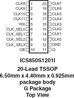
| 12:1 Single-Ended Multiplexer | Clock Multiplexers (MUX) | -40 to 85°C | TSSOP | 20 | 6.5 x 4.4 x 1.0 |
| Low Skew,1-to-6,Differential-to-2.5V,3.3V LVPECL/ECL Fanout Buffer | Clock Buffers & Drivers | -40 to 85°C | TSSOP | 20 | 6.5 x 4.4 x 1.0 |
| Low Skew,1-to-2,Differential-to-2.5V,3.3V LVPECL/ECL Fanout Buffer | Clock Buffers & Drivers | -40 to 85°C | SOIC, TSSOP | 8 | 3.0 x 3.0 x 0.97, 4.9 x 3.9 x 1.5 |
| 12:1 Differential-to-3.3V,2.5V LVPECL Clock/Data Multiplexer | Clock Multiplexers (MUX) | -40 to 85°C | VFQFPN | 32 | 5.0 x 5.0 x 0.9 |
| Low Skew,1-to-5 Differential-to-2.5V,3.3V LVPECL/ECL Fanout Buffer | Clock Buffers & Drivers | -40 to 85°C | TSSOP | 20 | 6.5 x 4.4 x 1.0 |
| 2:1 Differential-to-LVPECL Multiplexer | Clock Multiplexers (MUX) | -40 to 85°C | TSSOP, VFQFPN | 16 | 3.0 x 3.0 x 1.0, 5.0 x 4.4 x 1.0 |
| 4:1 Differential-to-3.3V, 2.5V LVPECL / ECL Clock Multiplexer | Clock Multiplexers (MUX) | -40 to 85°C | TSSOP | 20 | 6.5 x 4.4 x 1.0 |
| Low Skew, 1-to-10 Differential-to-2.5V, 3.3V LVPECL / ECL Fanout Buffer | Clock Buffers & Drivers | -40 to 85°C | VFQFPN | 32 | 5.0 x 5.0 x 0.9 |
| Low Skew,1-to-12,Differential-to-3.3V,2.5V LVPECL Fanout Buffer | Clock Buffers & Drivers | -40 to 85°C | VFQFPN | 32 | 5.0 x 5.0 x 0.9 |
| 2:1 Differential-to-LVDS Multiplexer | Clock Multiplexers (MUX) | -40 to 85°C | VFQFPN | 16 | 3.0 x 3.0 x 1.0 |
| 4:1 Differential-to-LVDS Clock Multiplexer | Clock Multiplexers (MUX) | -40 to 85°C | TSSOP | 16 | 5.0 x 4.4 x 1.0 |
| 8:1 Differential-to-LVDS Clock Multiplexer | Clock Multiplexers (MUX) | -40 to 85°C | TSSOP | 24 | 7.8 x 4.4 x 1.0 |
| Crystal or Differential to LVCMOS/ LVTTL Clock Buffer | Clock Buffers & Drivers | -40 to 85°C | VFQFPN | 32 | 5.0 x 5.0 x 0.9 |
| Crystal or Differential to LVCMOS/ LVTTL Clock Buffer | Clock Buffers & Drivers | -40 to 85°C | VFQFPN | 24 | 4.0 x 4.0 x 0.9 |
| Crystal or Differential to LVCMOS/ LVTTL Clock Buffer | Clock Buffers & Drivers | -40 to 85°C | VFQFPN | 32 | 5.0 x 5.0 x 0.9 |
| 1:2 LVDS 1.8V / 2.5V Fanout Buffer for 1PPS and High-Speed Clocks | RF Buffers | -40 to 85°C | VFQFPN | 16 | 3.0 x 3.0 x 1.0 |
| 1:6 LVDS Output 1.8V Fanout Buffer | RF Buffers | -40 to 85°C | VFQFPN | 20 | 4.0 x 4.0 x 1.0 |
| 2:4 LVDS 1.8V / 2.5V Fanout Buffer for 1PPS and High-Speed Clocks | RF Buffers | -40 to 85°C | VFQFPN | 16 | 3.0 x 3.0 x 1.0 |
| 2:8 LVDS 1.8V / 2.5V Fanout Buffer for 1PPS and High-Speed Clocks | RF Buffers | -40 to 85°C | VFQFPN | 28 | 5.0 x 5.0 x 0.8 |
| 2:12 LVDS 1.8V / 2.5V Fanout Buffer for 1PPS and High-Speed Clocks | RF Buffers | -40 to 85°C | VFQFPN | 40 | 6.0 x 6.0 x 0.9 |
| Dual 1:2 LVDS 1.8V / 2.5V Fanout Buffer for 1PPS and High-Speed Clocks | RF Buffers | -40 to 85°C (Tc ≤ 105°C) | VFQFPN | 16 | 3.0 x 3.0 x 1.0 |
| Dual 1:4 LVDS 1.8V / 2.5V Fanout Buffer for 1PPS and High-Speed Clocks | RF Buffers | -40 to 85°C (Tc ≤ 105°C) | VFQFPN | 28 | 5.0 x 5.0 x 0.8 |
| Dual 1:6 LVDS Output 1.8V / 2.5V Fanout Buffer | RF Buffers | -40 to 85°C (Tc ≤ 105°C) | WLCSP | 48 | 3.59 x 3.04 x 0.6 |
| Dual 1:6 LVDS Output 1.8V / 2.5V Fanout Buffer | RF Buffers | -40 to 85°C | VFQFPN | 40 | 6.0 x 6.0 x 0.9 |
| Dual 1:8 LVDS 1.8V / 2.5V Fanout Buffer for 1PPS and High-Speed Clocks | RF Buffers | -40 to 85°C (Tc ≤ 105°C) | VFQFPN | 48 | 7.0 x 7.0 x 0.9 |
| Low Additive Jitter 2:8 Buffer with Universal Differential Outputs | Clock Buffers & Drivers | -40 to 85°C | VFQFPN | 32 | 5.0 x 5.0 x 0.9 |
| Low Additive Jitter 2:8 Buffer with CMOS / Differential Outputs | Clock Buffers & Drivers | -40 to 85°C | VFQFPN | 32 | 5.0 x 5.0 x 0.9 |
| Programmable Low Additive Jitter 2:8 Buffer with Dividers and Universal Outputs | Clock Buffers & Drivers | -40 to 85°C | VFQFPN | 32 | 5.0 x 5.0 x 0.9 |
| 2:4, LVDS Output Fanout Buffer, 2.5V | RF Buffers | -40 to 85°C | VFQFPN | 16 | 3.0 x 3.0 x 1.0 |
| 2:4, LVDS Output Fanout Buffer, 3.3 V | RF Buffers | -40 to 85°C | VFQFPN | 16 | 3.0 x 3.0 x 1.0 |
| 1:8, LVDS Output Fanout Buffer | RF Buffers | -40 to 85°C | VFQFPN | 28 | 5.0 x 5.0 x 0.8 |
| 1:12, LVDS Output Fanout Buffer | RF Buffers | -40 to 85°C | VFQFPN | 40 | 6.0 x 6.0 x 0.9 |
| News | Apr 14, 2022 |
