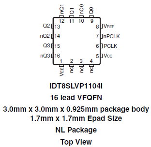
Low Phase Noise,1-to-4, 3.3V, 2.5V LVPECL Output Fanout Buffer
Overview
Description
Features
-
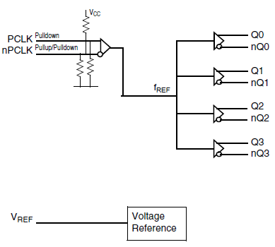
Four low skew, low additive jitter LVPECL differential output pairs
-
Differential LVPECL input pair can accept the following differential input levels: LVDS, LVPECL, CML
-
Differential PCLKx pairs can also accept single-ended LVCMOS levels. See the Applications section Writing the Differential Input Levels to Accept Single-ended Levels (Figures 1 and 2)
-
Maximum input clock frequency: 2GHz
-
LVCMOS interface levels for the control input (input select)
-
Output skew: 5ps (typical)
-
Propagation delay: 320ps (maximum)
-
Low additive phase jitter, RMS; fREF = 156.25MHz, VPP = 1V, 12kHz - 20MHz: 40fs (maximum)
-
Maximum device current consumption (IEE): 60mA (maximum)
-
Full 3.3V or 2.5V supply voltage
-
Lead-free (RoHS 6) packaging
-
-40°C to 85°C ambient operating temperature
Comparison
Applications
Design & Development
Software & Tools
Models
ECAD Models
Schematic symbols, PCB footprints, and 3D CAD models from SamacSys can be found by clicking on products in the Product Options table. If a symbol or model isn't available, it can be requested directly from the website.

Videos & Training
Description
Overview of IDT's 8LSVP (LVPECL) and 8SLVD (LVDS) families of low-jitter fanout buffers from IDT. Fanout buffers are a useful building block of many clock trees, providing signal buffering and multiple low-skew copies of the input signal. IDT's high-performance, low additive phase noise, differential clock fan-out buffers offer up to 2 GHz clock operation, low additive phase jitter (12kHz - 20MHz) of 50 to 100 femtoseconds RMS max, fast output rise & fall times (less than 150ps), and single and dual channel functions (dual: matched propagation delay). Presented by Baljit Chandhoke, Product Marketing Manager at Integrated Device Technology, Inc. To learn more about IDT's industry-leading portfolio of fanout buffers, visit Renesas's RF Buffer page.
Transcript


