
Realizes 40 Percent Reduced Mounting Area
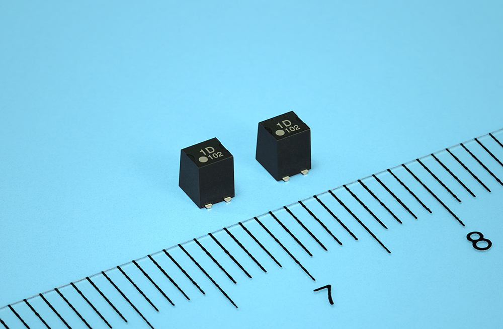 Compact Package Optical-Coupled MOSFET PS7901D-1A
TOKYO, Japan, January 31, 2010 — Renesas Electronics Corporation (TSE: 6723), a premier provider of advanced semiconductor solutions, today announced the development of an optical-coupled metal-oxide-semiconductor field-effect transistor (MOSFET), the PS7901D-1A, that achieves complete electrical isolation within the package by using light for signal transmission.
The PS7901D-1A device features an industry-leading ultra-compact 4-pin flat-lead package measuring only 2.9 millimeters (mm) × 2.3 mm, which is 40 percent smaller than that of Renesas Electronics' existing PS78 Series products, while retaining a guaranteed isolation voltage of 500 volts (V) r.m.s., equivalent to the company's existing products. The MOSFET chip inside the package combines low output capacitance and low leakage current. The extremely low leakage current when in the off state makes the PS7901D-1A suitable for high-frequency signal control in applications such as IC testers.
An optical-coupled MOSFET device combines in a single package three different elements: on the input side a light-emitting diode (LED) that converts an electrical signal into light, on the output side a photo voltaic diode (PVD) that converts light into an electrical signal, and an output MOSFET. The use of light to transmit the signal means that the input and output sides are completely isolated from each other electrically. This type of device is also referred to as a solid state relay (SSR). In contrast to mechanical relays, semiconductor relays are not subject to malfunction due to worn contacts or contamination by foreign matter. For this reason, mechanical relays are being replaced by solid state relay (SSR) in a wide range of applications, including IC testers, factory automation equipments, electric household appliances, and communication equipments.
Recently, demand has grown in the measuring equipment market for solid state relay (SSR) that are more compact and capable of operation at higher speeds as the trend in the devices being tested moves toward higher speed, better performance, and higher pin counts as part of a general tendency toward improved performance and processing power. IC testers especially incorporate a large number of switches for signal switching, and there is demand for compact and high-speed optical-coupled MOSFETs for use in such products to achieve reduced equipment size and better performance. Nevertheless, reducing the package size of optical-coupled MOSFETs involves solving the extremely difficult challenge of both maintaining sufficient isolation distance (Note 1) to ensure adequate isolation voltage and achieving high optical coupling efficiency (Note 2).
The PS7901D-1A device satisfies the above requirements and contributes to the development of equipment that combines compact size and excellent performance.
Key features of the PS7901D-1A device:
(1) Industry-leading compact package with approximately 40 percent reduced mounting area
The internal structure of the package incorporates improvements that draw on technology accumulated over many years of development work on photocouplers and optically-coupled MOSFET devices. Changing the structure inside the package from one in which the right and left lead frames are of different heights to one in which the lead frames face each other made it possible to achieve a smaller package size while maintaining the necessary distance and angle between the light-emitting and light-receiving elements. The resulting mounting area of 2.9 mm × 2.3 mm is approximately 40 percent smaller than that of Renesas Electronics' existing products with a compact flat-lead package (4.6 mm × 2.5 mm), while the same isolation voltage of 500 V r.m.s. is maintained.
(2) Industry-leading low output capacitance of 0.75 picofarads (pF)
The MOSFET used as an output element employs Renesas Electronics' exclusive silicon-on-insulator (SOI) technology. This enables an output capacitance of only 0.75 pF, among the lowest in the industry. An issue with MOSFETs is signal component leakage via the output capacitance when in the current-off state. The output capacitance of the PS7901D-1A is about 25 percent lower than the 1 pF of Renesas Electronics' existing compact-package products. This makes it possible to suppress signal component leakage and makes the PS7901D-1A device suitable for high-frequency operation.
(3) 70 percent lower leakage current
Through optimization of the gate film structure of the MOSFET, leakage current is reduced by 70 percent from the 100 picoamperes (pA) of existing Renesas Electronics products to 30 pA. This contributes to equipment with high measuring precision.
Renesas Electronics considers the PS7901D-1A device to be suitable for a wide range of applications where compactness and thin form factor are desirable, including measuring equipment such as IC testers, factory automation equipment, and office equipment.
Please refer to the separate sheet for the main specifications of the PS7901D-1A.
(Note 1) Isolation distance:
The distance between the pght-emitting and pght-receiving elements.
(Note 2) Optical coupling efficiency:
The pght transmittance between the pght-emitting and pght-receiving elements.
Pricing and Availability
Samples of Renesas Electronics' PS7901D-1A device are available now priced at US$2.5. Mass production is scheduled to begin in the first half of FY2011 and is expected to reach a production volume of 1,000,000 units per month. (Pricing and availability are subject to change without notice.)
(Remarks)
All other registered trademarks or trademarks are the property of their respective owners.
About Renesas Electronics Corporation
Renesas Electronics Corporation (TSE: 6723) delivers trusted embedded design innovation with complete semiconductor solutions that enable billions of connected, intelligent devices to enhance the way people work and live. A global leader in microcontrollers, analog, power and SoC products, Renesas provides comprehensive solutions for a broad range of automotive, industrial, infrastructure, and IoT applications that help shape a limitless future. Learn more at renesas.com. Follow us on LinkedIn, Facebook, Twitter, and YouTube.
The content in the press release, including, but not limited to, product prices and specifications, is based on the information as of the date indicated on the document, but may be subject to change without prior notice.