
 New eDRAM structure
TOKYO, Japan, December 9, 2010 — Renesas Electronics Corporation (TSE: 6723), a premier provider of advanced semiconductor solutions, today announced the development of a basic structure for embedded DRAM (eDRAM) highly compatible with standard logic circuit design assets (IP: intellectual property) of the next generation system LSIs at the 28-nanometer (nm) node and beyond.
Due to the increasingly widespread use of digital TVs, digital still cameras and game consoles that produce high image quality, there is a growing demand for a technology that realizes higher-speed processing capability and low power consumption for consumer electronic devices and high-performance servers and networking devices. To address these needs, Renesas Electronics has been providing eDRAM products that achieve both high-speed processing and low power consumption and has shipped more than 200,000,000 units.
To assure both stable memory operation and sufficient data retention times, the capacitors used for the DRAM are formed after transistors have been formed on a silicon substrate, and finally the interconnects that connect these devices are formed on top of the eDRAM structure. As a result, in the logic circuit areas where no DRAM capacitors are formed, it is necessary to connect the transistors and interconnects through long “bypass contacts” that have the same height as the capacitors. However, as miniaturization progresses, it becomes necessary to reduce the diameter of and spacing between those bypass contacts. This makes it impossible to ignore the influence of the increasing resistance and parasitic capacitance of the bypass contacts and, unlike previous generations, it is difficult to reuse the IP developed for use in standard CMOS logic circuit without the bypass contacts.
Renesas Electronics has developed a new structure that embeds the DRAM capacitors and interconnects in the same layer by using improvements to the dielectric material and other aspects as a means for overcoming technological issues, and thereby has achieved significantly improved compatibility with ordinary system LSI manufacturing processes.
This new technology embeds the capacitors, which are the data storage elements in DRAM, in the interconnect layer used for the logic circuits. As a result, it will be possible to create embedded memory that seamlessly combines the globally standardized logic circuit IP with Renesas Electronics' advanced eDRAM technology. Adoption of this new technology will also lead to more efficient and lower cost development of leading-edge devices to be fabricated at the 28-nm node and beyond.
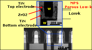
Key features of the newly developed technology:
(1) By embedding the cylindrical capacitors in the interconnect layer instead of forming a layer independent of the interconnect layer, this new technology obviates the need for the long bypass contacts that were formed between the logic area transistors and the interconnect layer. The parasitic capacitance and parasitic resistance due to the bypass contacts is reduced, thus preventing degradation of logic circuit performance. As a result, it is now possible to design eDRAM even at the 28-nm node and beyond using IP developed for use in standard 28-nm node CMOS logic.
(2) By adopting the unique molecular pore stack (MPS) film for the interconnect layer, diffusion of metal electrode material into the porous low-k film attached to the capacitor sidewalls is suppressed. As a result, Renesas Electronics has succeeded in assuring dielectric reliability of over 10 years for the porous low-k film between 50-nm-spaced capacitors needed for the 28-nm node eDRAM.
The newly developed technology reduces the parasitic capacitance and parasitic resistance that have become problems in the development of leading-edge LSIs fabricated in the 28nm node and later processes by embedding capacitors in the interconnect layer and obviating the need for bypass contacts. This makes it possible to make use of IP developed for use in standard CMOS logic.
On the other hand, a porous film is used as the interlayer dielectric in leading-edge LSIs to achieve both higher speeds and low power consumption. Therefore, when forming capacitors within the interconnect layer, porous dielectric film between interconnect layers are contaminated easily by diffusion of electrode materials, which degrade the dielectric reliability. While the capacitor electrodes are formed in this porous film using gas-phase deposition, there is concern that the gas-phase material will infiltrate through the pores in the dielectrics and degrade performance.
Pore size control technology is essential in solving this problem. By adopting the MPS film with a sub-nanometer-size closed-pore structure film, Renesas Electronics has restricted the entry of the metallic electrode material into the porous film. Additionally, by combining this technology with surface-absorption-type CVD process, Renesas Electronics has succeeded in perfectly eliminating metal contamination into the MPS film. Renesas Electronics has verified that a dielectric film lifetime of over 10 years could be guaranteed in 50-nm space.
Renesas Electronics' new eDRAM technology makes it possible both to create ICs that seamlessly combine the globally standardized CMOS logic IP with Renesas Electronics' eDRAM technology at the 28-nm node and beyond, and also to achieve higher speeds and lower power consumption in the DRAM/logic interface. Renesas Electronics is working to apply this technology as soon as possible and will continue to push forward with research and development in this area.
Renesas Electronics presented the results of this research at the International Electron Devices Meeting 2010 (IEDM 2010), which was held from December 6 through December 8 in San Francisco, U.S.
(Remarks)
All registered trademarks or trademarks are the property of their respective owners.
About Renesas Electronics Corporation
Renesas Electronics Corporation (TSE: 6723) delivers trusted embedded design innovation with complete semiconductor solutions that enable billions of connected, intelligent devices to enhance the way people work and live. A global leader in microcontrollers, analog, power and SoC products, Renesas provides comprehensive solutions for a broad range of automotive, industrial, infrastructure, and IoT applications that help shape a limitless future. Learn more at renesas.com. Follow us on LinkedIn, Facebook, Twitter, and YouTube.
The content in the press release, including, but not limited to, product prices and specifications, is based on the information as of the date indicated on the document, but may be subject to change without prior notice.