
ZVS Full-Bridge PWM Controller Evaluation Board
跳转至页面部分:
概览
简介
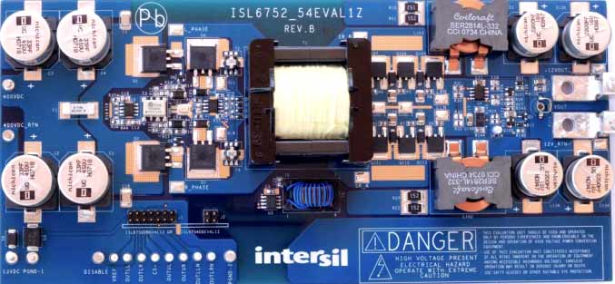
The ISL6752/54EVAL1Z is a new design based on the ISL6752EVAL1Z but with several design modifications to improve the efficiency from 90% to 95%. The control circuit has been moved off the main board onto a daughter card. Two different daughter cards are provided: one using the ISL6752 and the other using the ISL6754. Both control cards utilize the Renesas zero voltage switching (ZVS) topology. The ISL6752 daughter card features pulse by pulse current limiting, and the ISL6754 daughter card features a patented method for average current limiting that results in a brick-wall current limit profile.
The PCB layout of the ISL6752/54EVAL1Z has also been greatly improved over the ISL6752EVAL1Z. Even though the overall size of the board has been reduced, the copper losses have been reduced.
In addition to the ZVS function, this board also incorporates N-Channel FETs as secondary side rectifiers, also known as synchronous rectifiers (SR). Power dissipation of the secondary side rectifiers is reduced because the conduction losses of SRs are significantly less than the conduction losses of PN or Schottky diodes.
特性
- Absolute maximum input voltage 450VDC
- Operating input voltage 350V to 450VDCC
- Maximum input current 2.5ADC
- Rated output current 50ADC
- Current limit 60A ± 5%
- Output voltage 12V ± 5%
- Efficiency at 100% (50A) load 95%
- Efficiency at 20% (10A) load 92%
应用
应用
- ZVS full-bridge converters
- Telecom and datacom power
- Wireless basestation power
- File server power
- Industrial power systems
Processing table

Tips for Using This Parametric Table:
- Hide Filters button in header: Collapse or expands filters
- Column sort buttons in header: Sort Column alphabetically / numerically descending or ascending
- Reset button in header: Reset all filters to the page default
- Full Screen button in header: Expand the table to full screen view (user must close out of full screen before they can interact with rest of page)
- Export button in header: Export the filtered results of the table to an Excel document
- Filter parts search bar in header: Type to filter table results by part number
- Hide column button in column headers: Select to hide columns in table
- AND / OR toggle switches in header: Toggles the logic of this particular filter to be “AND” or “OR” logic for filtering results
- Multiselect checkboxes at beginning of each row in table: Select these checkboxes to compare products against each other
- Document icon next to product name in row: View the featured document for this product
- Chip icon next to the right of the document icon in row: View the block diagram for this product
- Cart icon to the right of the chip icon: Indicates that samples are available for this product