
Overview
Description
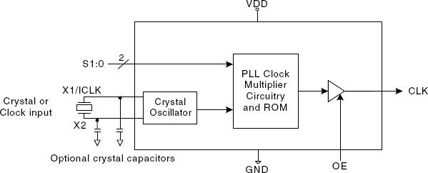
The 501A is the most cost effective way to generate a high quality, high frequency clock output from a lower frequency crystal or clock input. It is designed to replace crystal oscillators in most electronic systems. Using Phase-Locked Loop (PLL) techniques, the device uses a standard fundamental mode, inexpensive crystal to produce output clocks up to 200 MHz. Stored in the chip's ROM is the ability to generate nine different multiplication factors, allowing one chip to output many common frequencies (see table on page 2). The device also has an output enable pin which tri-states the clock output when the OE pin is taken low. This product is intended for clock generation. It has low output jitter (variation in the output period), but input to output skew and jitter are not defined or guaranteed. For applications which require defined input to output skew, use the 570B.
Features
- Packaged as 8-pin SOIC (Pb-free) or die
- IDT's lowest cost PLL clock
- Zero ppm multiplication error
- Input crystal frequency of up to 27 MHz
- Input clock frequency of up to 50 MHz
- Output clock frequencies up to 200 MHz
- Extremely low jitter of 25 ps (one sigma)
- Compatible with all popular CPUs
- Duty cycle of 45/55 up to 200 MHz
- Nine selectable frequencies
- Operating voltage of 3.3 V
- Tri-state output for board level testing
- 25 mA drive capability at TTL levels
- Ideal for oscillator replacement
- Optimized for output frequencies of up to 200 MHz (166 MHz maximum for industrial temperature version)
- Industrial temperature version available
- Advanced, low power CMOS process
Comparison
Applications
Design & Development
Models
ECAD Models
Schematic symbols, PCB footprints, and 3D CAD models from SamacSys can be found by clicking on products in the Product Options table. If a symbol or model isn't available, it can be requested directly from the website.

Processing table
| WAFER | 0 | C | Yes | Wafer | ||
| SOIC | 8 | I | Yes | Tube | ||
| SOIC | 8 | I | Yes | Reel | ||
| SOIC | 8 | C | Yes | Tube | ||
| SOIC | 8 | C | Yes | Reel |

Tips for Using This Parametric Table:
- Hide Filters button in header: Collapse or expands filters
- Column sort buttons in header: Sort Column alphabetically / numerically descending or ascending
- Reset button in header: Reset all filters to the page default
- Full Screen button in header: Expand the table to full screen view (user must close out of full screen before they can interact with rest of page)
- Export button in header: Export the filtered results of the table to an Excel document
- Filter parts search bar in header: Type to filter table results by part number
- Hide column button in column headers: Select to hide columns in table
- AND / OR toggle switches in header: Toggles the logic of this particular filter to be “AND” or “OR” logic for filtering results
- Multiselect checkboxes at beginning of each row in table: Select these checkboxes to compare products against each other
- Document icon next to product name in row: View the featured document for this product
- Chip icon next to the right of the document icon in row: View the block diagram for this product
- Cart icon to the right of the chip icon: Indicates that samples are available for this product