
New NFC-based Technology Achieves Wider Charging Area and Smaller Footprint in Consumer Products such as Smartphones and Healthcare Devices. By Providing a Complete Development Kit Renesas Contributes to Shortening the System Development Cycle.
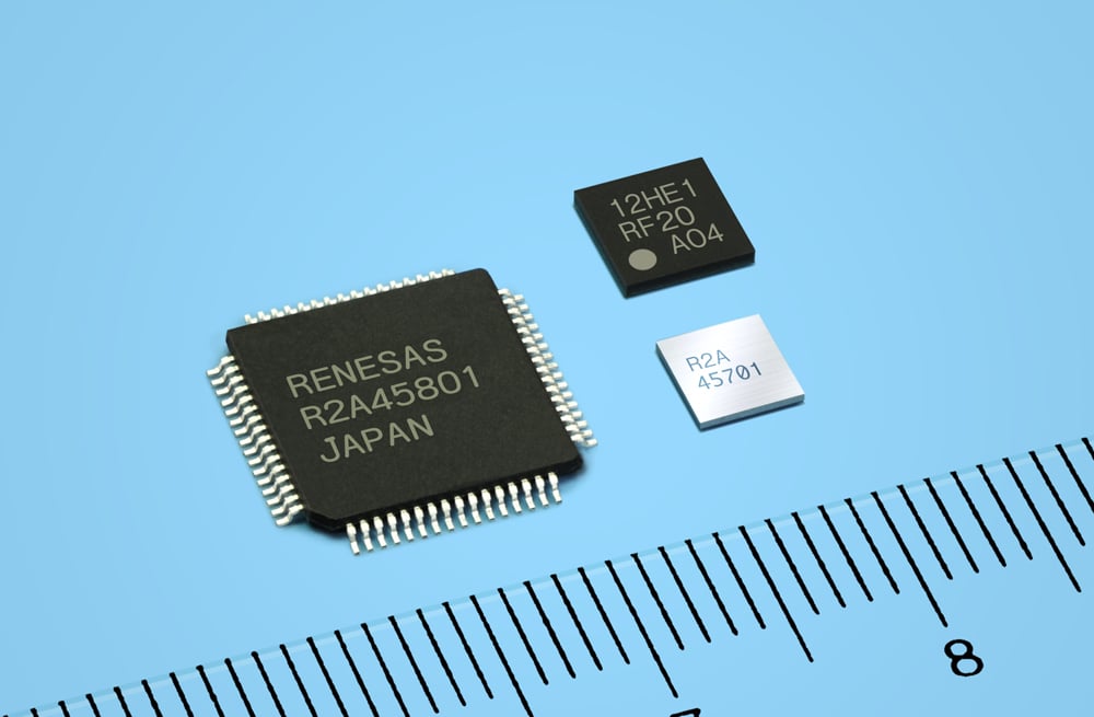 Renesas Electronics NFC wireless charging system solution
TOKYO, Japan, September 12, 2012 — Renesas Electronics Corporation (TSE: 6723), a premier supplier of advanced semiconductor solutions, has developed the near field communication (NFC) (Note 1) wireless charging system to eliminate the power cable for charging and increase efficiency of those systems. Renesas supplies the essential components needed to build a system: the NFC microcontroller (MCU) RF20, the power transmitter IC R2A45801, and the power receiver IC R2A45701. Renesas also provides the total kit including peripheral general-purpose devices (e.g. power semiconductor devices) as a system solution.
Wireless charging is starting to become popular in products such as smartphones. It eases battery charging of portable devices and makes cables and connectors redundant. Today's existing wireless charging systems typically couple two antennas, one for receiving and one for transmitting power. The gap between and the combination of the two antennas highly influence the efficiency of the charging power. Such existing wireless charging systems limit the effective charging area significantly. In consequence the alignment of the transmitting and receiving antennas greatly reduces the freedom of product design.
The Renesas NFC wireless charging technology widens the charging area to about 10 cm. It incorporates the technology of the existing NFC MCU, and utilizes the NFC antenna to implement a wireless charging system that uses a single RX antenna for NFC communication and receiving power, thereby improving reliability while reducing the bill of material of a receiver design. To make it easier for developers to incorporate this system into their mobile devices, Renesas developed the NFC MCU, the power receiver IC, and the power transmitter IC built around the company's proven power technology. These new products are the main components necessary to implement a wireless charging system and are supplied as a total solution kit.
Key Features of the Renesas' Wireless Charging System
The NFC wireless charging system solution not only makes the charging cable-free, but also makes it possible to achieve a new, more flexible level of wireless connectivity by fusing NFC and wireless charging technology. The main features of the system are described below.
1) Power transmission and data reception via a single antenna with NFC
Conventional wireless power receiver with additional short range communication capabilities requires two antennas, one for data transmission and one for receiving power. In an NFC-based system the receiver uses a single antenna, contributing to more compact and thinner mobile handsets.
2) Expansion of charging area with NFC
The exclusive technology employing NFC makes it possible to widen the charging area to about 10 cm, making it possible to build a wireless charging system relatively unaffected by positioning deviation. The flexibility in mobile handset power receiver positioning allows more flexible design for handsets and power transmitters.
3) Ability to build wireless charging systems with a high level of safety
NFC supports bi-directional intercommunication, so it is possible to verify (determine) whether a device can be charged before the supply of power begins. This increases the safety of the wireless charging.
4) A single NFC MCU for both wireless charging and conventional contactless smart card applications
Based on the NFC standard, the system supports not only wireless power supplies but also existing contactless smart card applications. This enables the designing of more compact mobile handsets.
Renesas has submitted the new solution to the Wireless Charging Task Force of the NFC Forum (Note 2) as part of encouraging the broad adoption of NFC wireless charging systems.
An overview of the three new products and their main features is provided below.
NFC Controller RF20
In addition to wireless charging applications, NFC can be used for a wide variety of other applications, including conventional ones such as payment transactions, transportation systems, and ticketing, as well as newer ones such as gaming and healthcare devices. In particular, smartphones based on the Android™ OS and equipped with NFC functions are proliferating rapidly. This has spurred demand for solutions for easy implementation of NFC functionality. In response, Renesas has developed the RF20 NFC MCU to be compliant with the international NFC standards and with support for smartphones based on the Android™ OS.
1) Turnkey solutions
The chip is supplied with the programmed firmware incorporating all the functions required by smartphones and other devices, including a validation function for compatibility of the various NFC standards, with middleware for the host side. This makes it possible to implement NFC functions quickly and easily on Android™ devices.
2) Support for a variety of interface standards
Single Wire Protocol (SWP) (ETSI TS 102 613 compliant) is provided as a communication interface to external secure elements required for applications such as payment transactions, and can be also connected to an SIM card (Note 3). In addition, inter-integrated circuit (I2C) and universal asynchronous receiver/transmitter (UART) are supported as host controller interfaces. This enables flexible configuration of different host interface types.
Power transmitter IC R2A45801 and power receiver IC R2A45701 for wireless power supplies
The main analog components required to configure a wireless charging system are integrated into single-chip products.
1) Features of power transmitter IC R2A45801
Power transmitter IC R2A45801 implements the three charging output channels required in the driver circuit of a wireless power transmitter. It also has on-chip functions for enhanced control safety, including thermal shutdown and field effect transistor (FET) temperature detection/system temperature detection functions. When employed in conjunction with RJK1028 external Metal-Oxide-Semiconductor Field-Effect Transistors (MOSFETs), power transmitter IC R2A45801 can be used to build a highly efficient power transmission system.
2) Features of power receiver IC R2A45701
Power receiver IC R2A45701 steps down the voltage received by the coil on the receiver side after rectification to the specified level required for charging control. It also has voltage and current monitoring functions as well as an AC adapter input, a USB charging input, and an input for external charging other than wireless charging. Supporting these multiple charging inputs is an on-chip charging control function that enables direct charging of a single-cell lithium-ion battery. Hence the R2A45701 provides standalone support for devices incorporating a battery.
(Note 1) Near field communication (NFC) is an international short-range wireless communication standard using the 13.56 MHz frequency band that was developed by NXP Semiconductors and Sony Corporation.
(Note 2) NFC Forum: An industry association devoted to the development of NFC standard specifications and promoting the widespread adoption of NFC products. As a sponsor member of the NFC Forum, Renesas is working to promote the spread of NFC technology.
(Note 3) SIM card: SIM stands for Subscriber Identity Module, an integrated circuit card (ICC) storing subscriber information such as the telephone number issued by the mobile phone carrier.
Refer to the separate sheet for the main specifications of the NFC MCU RF20, power transmitter IC R2A45801, and power receiver IC R2A45701.
Pricing and Availability
Samples of the NFC MCU RF20, power transmitter IC R2A45801 and receiver IC R2A45701 will be available in November 2012, priced at US$6.00 per unit for NFC MCU RF20, US$6.00 per unit for transmission IC R2A45801, and US$6.00per unit for power receiver IC R2A45801. Mass production of NFC MCU RF20 is scheduled to begin in January 2013 and is expected to reach a scale of 1,000,000 units per month in June 2013. Mass production of power transmitter IC R2A45801 and power receiver IC R2A45701 is scheduled to begin in March 2013 and is expected to reach a scale of 1,000,000 units per month in December 2013. (Pricing and availability are subject to change without notice.)
(Remarks)
“Android” is a trademark of Google Inc. Other names of products or services mentioned in this press release are trademarks or registered trademarks of their respective owners.
About Renesas Electronics Corporation
Renesas Electronics Corporation (TSE: 6723) delivers trusted embedded design innovation with complete semiconductor solutions that enable billions of connected, intelligent devices to enhance the way people work and live. A global leader in microcontrollers, analog, power, and SoC products, Renesas provides comprehensive solutions for a broad range of automotive, industrial, infrastructure, and IoT applications that help shape a limitless future. Learn more at renesas.com. Follow us on LinkedIn, Facebook, Twitter, and YouTube.
The content in the press release, including, but not limited to, product prices and specifications, is based on the information as of the date indicated on the document, but may be subject to change without prior notice.