High Speed A/D Converter Evaluation Kits
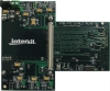
Renesas offers two options for evaluating high-speed analog-to-digital converter products with LVDS and/or LVCMOS outputs. A complete, turnkey evaluation platform is...

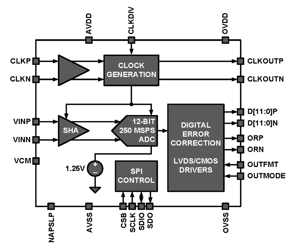
The ISLA112P25MREP is a low-power 12-bit, 250MSPS analog-to-digital converter. Designed with Renesas' proprietary FemtoCharge™ technology on a standard CMOS process. A serial peripheral interface (SPI) port allows for extensive configurability, as well as fine control of various parameters such as gain and offset. Digital output data is presented in selectable LVDS or CMOS formats. The ISLA112P25MREP is available in a 72 Ld QFN package with an exposed paddle. Operating from a 1. 8V supply, performance is specified over the full military temperature range (-55°C to +125°C).
|
|
|
|
|---|---|---|
| 类型 | 文档标题 | 日期 |
| 数据手册 | PDF 882 KB | |
| 手册 | PDF 467 KB | |
| 手册 | PDF 4.85 MB | |
| 其他 | ||
| Product Advisory | PDF 282 KB | |
| 应用文档 | PDF 338 KB | |
| 应用文档 | PDF 503 KB | |
| 应用文档 | PDF 1.08 MB | |
| 应用文档 | PDF 287 KB | |
9 items
|
||
Renesas offers two options for evaluating high-speed analog-to-digital converter products with LVDS and/or LVCMOS outputs. A complete, turnkey evaluation platform is...
Schematic symbols, PCB footprints, and 3D CAD models from SamacSys can be found by clicking on products in the Product Options table. If a symbol or model isn't available, it can be requested directly from the website.

| QFN | Tray | 69 | 3 |
