19-output Differential Buffer For PCIe Gen3
Jump to Page Section:
Overview
Description
The 9DB1933 zero-delay buffer supports PCIe Gen3 requirements, while being backwards compatible to PCIe Gen2 and Gen1. The 9DB1933 is driven by a differential SRC output pair from an IDT 932S421, 932SQ420, or equivalent, main clock generator. It attenuates jitter on the input clock and has a selectable PLL bandwidth to maximize performance in systems with or without Spread-Spectrum clocking.

Features
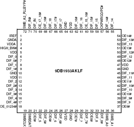
- 19 - 0.7 V current mode differential HCSL output pairs
- 8 Selectable SMBus Addresses/Multiple devices can share the same SMBus Segment
- 11 dedicated and 3 group OE# pins/Hardware control of the outputs
- PLL or bypass mode/PLL can dejitter incoming clock
- Selectable PLL bandwidth/minimizes jitter peaking in downstream PLL's
- Spread spectrum compatible, tracks spreading input clock for low EMI
- SMBus Interface, unused outputs can be disabled
- Supports undriven differential outputs in Power Down mode for power management
- Cycle-to-cycle jitter <50 ps
- Output-to-output skew < 150 ps
- PCIe Gen3 phase jitter < 1.0 ps RMS
Comparison
Applications
Design & Development
Models
ECAD Models
Schematic symbols, PCB footprints, and 3D CAD models from SamacSys can be found by clicking on products in the Product Options table. If a symbol or model isn't available, it can be requested directly from the website.

Processing table
| VFQFPN | 72 | C | Yes | Tray | ||
| VFQFPN | 72 | C | Yes | Reel |

Tips for Using This Parametric Table:
- Hide Filters button in header: Collapse or expands filters
- Column sort buttons in header: Sort Column alphabetically / numerically descending or ascending
- Reset button in header: Reset all filters to the page default
- Full Screen button in header: Expand the table to full screen view (user must close out of full screen before they can interact with rest of page)
- Export button in header: Export the filtered results of the table to an Excel document
- Filter parts search bar in header: Type to filter table results by part number
- Hide column button in column headers: Select to hide columns in table
- AND / OR toggle switches in header: Toggles the logic of this particular filter to be “AND” or “OR” logic for filtering results
- Multiselect checkboxes at beginning of each row in table: Select these checkboxes to compare products against each other
- Document icon next to product name in row: View the featured document for this product
- Chip icon next to the right of the document icon in row: View the block diagram for this product
- Cart icon to the right of the chip icon: Indicates that samples are available for this product
Videos & Training
PCIe Clocking Architectures (Common and Separate)

Video List
News & Blog Posts
| Blog Post | Apr 14, 2022 | ||
| Blog Post | May 22, 2018 | ||
| News | Apr 30, 2018 |