
Low Skew,1-to-24 Differential-to-LVCMOS/LVTTL Fanout Buffer
NOTICE - The following device(s) are recommended alternatives:
Jump to Page Section:
Overview
Description
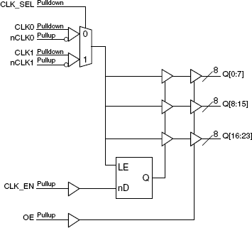
The 8344I-01 is a low voltage, low skew fanout buffer. The 8344I-01 has two selectable clock inputs. The CLKx, nCLKx pairs can accept most standard differential input levels. The 8344I-01 is designed to translate any differential signal level to LVCMOS/LVTTL levels. The low impedance LVCMOS/LVTTL outputs are designed to drive 50Ω series or parallel terminated transmission lines. The effective fanout can be increased to 48 by utilizing the ability of the outputs to drive two series terminated lines. Redundant clock applications can make use of the dual clock inputs which also facilitate board level testing. The clock enable is internally synchronized to eliminate runt pulses on the outputs during asynchronous assertion/deassertion of the clock enable pin. The outputs are driven low when disabled. The 8344I-01 is characterized at full 3.3V, full 2.5V and mixed 3.3V input and 2.5V output operating supply modes. Guaranteed output and part-to-part skew characteristics make the 8344I-01 ideal for those clock distribution applications demanding well defined performance and repeatability.
Features
- Twenty-four LVCMOS/LVTTL outputs, 7Ω typical output impedance
- Two selectable differential CLKx, nCLKx inputs
- CLK0, nCLK0 and CLK1, nCLK1 pairs can accept the following input levels: LVDS, LVPECL, LVHSTL, HCSL
- Maximum output frequency: 100MHz
- Translates any single ended input signal to LVCMOS/LVTTL with resistor bias on nCLK input
- Synchronous clock enable
- Additive phase jitter, RMS: 0.21ps (typical)
- Output skew: 200ps (maximum)
- Part-to-part skew: 900ps (maximum)
- Bank skew: 180ps (maximum)
- Propagation delay: 5ns (maximum)
- Output supply modes: Core/Output 3.3V/3.3V 2.5V/2.5V 3.3V/2.5V
- -40°C to 70°C ambient operating temperature
- Available in lead-free (RoHS 6) package
Comparison
Applications
Design & Development
Models
ECAD Models
Schematic symbols, PCB footprints, and 3D CAD models from SamacSys can be found by clicking on products in the Product Options table. If a symbol or model isn't available, it can be requested directly from the website.

Processing table
| TQFP | 48 | I | Yes | Tray | ||
| TQFP | 48 | I | Yes | Reel |

Tips for Using This Parametric Table:
- Hide Filters button in header: Collapse or expands filters
- Column sort buttons in header: Sort Column alphabetically / numerically descending or ascending
- Reset button in header: Reset all filters to the page default
- Full Screen button in header: Expand the table to full screen view (user must close out of full screen before they can interact with rest of page)
- Export button in header: Export the filtered results of the table to an Excel document
- Filter parts search bar in header: Type to filter table results by part number
- Hide column button in column headers: Select to hide columns in table
- AND / OR toggle switches in header: Toggles the logic of this particular filter to be “AND” or “OR” logic for filtering results
- Multiselect checkboxes at beginning of each row in table: Select these checkboxes to compare products against each other
- Document icon next to product name in row: View the featured document for this product
- Chip icon next to the right of the document icon in row: View the block diagram for this product
- Cart icon to the right of the chip icon: Indicates that samples are available for this product