
2.5V LVDS,1:6 Glitchless Clock Buffer Terabuffer™ II
NOTICE - The following device(s) are recommended alternatives:
Jump to Page Section:
Overview
Description
The 5T93GL06 2.5V differential clock buffer is a user- selectable differential input to six LVDS outputs. The fanout from a differential input to six LVDS outputs reduces loading on the preceding driver and provides an efficient clock distribution network. The 5T93GL06 can act as a translator from a differential HSTL, eHSTL, LVEPECL (2.5V), LVPECL (3.3V), CML, or LVDS input to LVDS outputs. A single-ended 3.3V / 2.5V LVTTL input can also be used to translate to LVDS outputs. The redundant input capability allows for a glitchless change-over from a primary clock source to a secondary clock source up to 650MHz. Selectable inputs are controlled by SEL. During the switchover, the output will disable low for up to three clock cycles of the previously-selected input clock. The outputs will remain low for up to three clock cycles of the newly-selected clock, after which the outputs will start from the newly-selected input. A FSEL pin has been implemented to control the switchover in cases where a clock source is absent or is driven to DC levels below the minimum specifications. The 5T93GL06 outputs can be asynchronously enabled/ disabled. When disabled, the outputs will drive to the value selected by the GL pin. Multiple power and grounds reduce noise.

Features
- Guaranteed low skew: <25ps (maximum)
- Very low duty cycle distortion: <100ps (maximum)
- High speed propagation delay: <2ns (maximum)
- Up to 800MHz operation
- Glitchless input clock switching up to 650MHz
- Selectable inputs
- Hot insertable and over-voltage tolerant inputs
- 3.3V/2.5V LVTTL, HSTL, eHSTL, LVEPECL (2.5V), LVPECL (3.3V), CML or LVDS input interface
- Selectable differential inputs to six LVDS outputs
- Power-down mode
- At power-up, FSEL should be LOW
- 2.5V VDD
- -40°C to 85°C ambient operating temperature
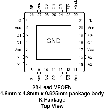
- Available in VFQFN package
- Recommends IDT5T9306 if glitchless input selection is not required
Comparison
Applications
Design & Development
Models
ECAD Models
Schematic symbols, PCB footprints, and 3D CAD models from SamacSys can be found by clicking on products in the Product Options table. If a symbol or model isn't available, it can be requested directly from the website.

Processing table
| VFQFPN | 28 | I | Yes | Tray |

Tips for Using This Parametric Table:
- Hide Filters button in header: Collapse or expands filters
- Column sort buttons in header: Sort Column alphabetically / numerically descending or ascending
- Reset button in header: Reset all filters to the page default
- Full Screen button in header: Expand the table to full screen view (user must close out of full screen before they can interact with rest of page)
- Export button in header: Export the filtered results of the table to an Excel document
- Filter parts search bar in header: Type to filter table results by part number
- Hide column button in column headers: Select to hide columns in table
- AND / OR toggle switches in header: Toggles the logic of this particular filter to be “AND” or “OR” logic for filtering results
- Multiselect checkboxes at beginning of each row in table: Select these checkboxes to compare products against each other
- Document icon next to product name in row: View the featured document for this product
- Chip icon next to the right of the document icon in row: View the block diagram for this product
- Cart icon to the right of the chip icon: Indicates that samples are available for this product