
2.5V Differential Clock Divider/Buffer
Jump to Page Section:
Overview
Description
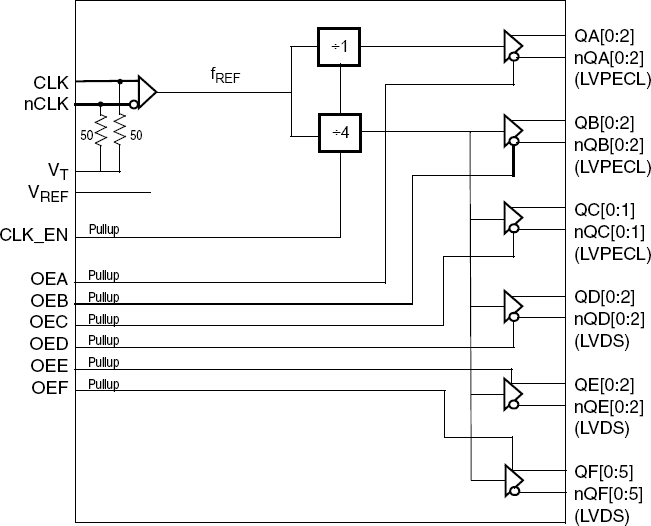
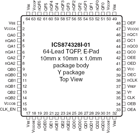
The 874328I-01 is a high-performance differential ÷1 and ÷4 clock divider and fanout buffer. The device is designed for the frequency-division and signal fanout of high-frequency, low phase-noise clock signals. The differential input signal is frequency divided by ÷1 and ÷4. Three LVPECL and three LVDS output banks are provided with a total of twenty differential outputs. The 874328I-01 is characterized to operate from a 2.5V power supply. Guaranteed output-to-output and part-to-part skew characteristics make the 874328I-01 ideal for those clock distribution applications demanding well-defined performance and repeatability.
Features
- One differential input LVPECL reference clock
- Differential pair can accept the following differential input levels: LVPECL, LVDS, CML, SSTL
- Integrated input termination resistors
- One bank of three LVPECL outputs (÷1 frequency-divided)
- One bank of three LVPECL outputs (÷4 frequency-divided)
- One bank of two LVPECL outputs (÷4 frequency-divided)
- Two banks of three LVDS outputs (÷4 frequency-divided)
- One bank of six LVDS outputs (÷4 frequency-divided)
- Total of twenty differential clock outputs
- Maximum input frequency: 650MHz
- Maximum output frequency: 650MHz (÷1 outputs)
- Maximum output frequency: 162.5MHz (÷4 outputs)
- LVCMOS interface levels for all control inputs
- Output skew: 70ps (maximum)
- Part-to-part skew: 250ps (maximum)
- Full 2.5V supply voltage
- Available in lead-free (RoHS 6) package
- -40°C to 85°C ambient operating temperature
Comparison
Applications
Design & Development
Models
ECAD Models
Schematic symbols, PCB footprints, and 3D CAD models from SamacSys can be found by clicking on products in the Product Options table. If a symbol or model isn't available, it can be requested directly from the website.

Processing table
| TQFP | 64 | I | Yes | Tray | ||
| TQFP | 64 | I | Yes | Reel |

Tips for Using This Parametric Table:
- Hide Filters button in header: Collapse or expands filters
- Column sort buttons in header: Sort Column alphabetically / numerically descending or ascending
- Reset button in header: Reset all filters to the page default
- Full Screen button in header: Expand the table to full screen view (user must close out of full screen before they can interact with rest of page)
- Export button in header: Export the filtered results of the table to an Excel document
- Filter parts search bar in header: Type to filter table results by part number
- Hide column button in column headers: Select to hide columns in table
- AND / OR toggle switches in header: Toggles the logic of this particular filter to be “AND” or “OR” logic for filtering results
- Multiselect checkboxes at beginning of each row in table: Select these checkboxes to compare products against each other
- Document icon next to product name in row: View the featured document for this product
- Chip icon next to the right of the document icon in row: View the block diagram for this product
- Cart icon to the right of the chip icon: Indicates that samples are available for this product