
2.5V,3.3V ECL/LVPECL Clock /Data Fanout Buffer
Jump to Page Section:
Overview
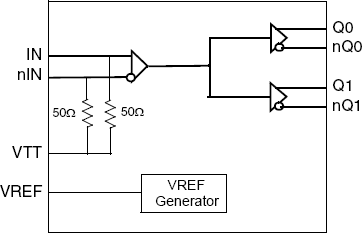
Description
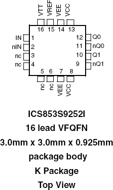
The 853S9252I is a 2.5V/3.3V ECL/LVPECL fanout buffer designed for high-speed, low phase-noise wireless infrastructure applications. The device fanouts a differential input signal to two ECL/LVPECL outputs. Optimized for low additive phase-noise, sub-100ps output rise and fall times, low output skew and high-frequencies, the 853S9252I is an effective solution for high-performance clock and data distribution applications, for instance driving the reference clock inputs of ADC/DAC circuits. Internal input termination, a bias voltage output (VREF) for AC-coupling and small packaging (3.0mm x 3.0mm 16-lead VFQFN) supports space-efficient board designs. The 853S9252I operates from a full 2.5V or 3.3V power supply and supports the industrial temperature range of -40°C to 85°C. The extended temperature range also supports wireless infrastructure, tele-communication and networking end equipment requirements.
Features
- 1:2 differential clock/data fanout buffer
- Clock frequency: 3GHz (maximum)
- Two differential 2.5V/3.3V ECL/LVPECL clock output
- Differential input accepts ECL/LVPECL, LVDS and CML levels
- Additive phase jitter, RMS @ 122.88MHz: 45fs (typical)
- Propagation delay: 175ps (maximum), VCC = 3.3V
- Output rise/fall time: 135ps (maximum), VCC = 3.3V
- Internal input signal termination
- Supply voltage: 2.5V-5% to 3.3V+10%
- Available in Lead-free (RoHS 6) package
- -40°C to 85°C ambient operating temperature
Comparison
Applications
Design & Development
Models
ECAD Models
Schematic symbols, PCB footprints, and 3D CAD models from SamacSys can be found by clicking on products in the Product Options table. If a symbol or model isn't available, it can be requested directly from the website.

Processing table
| VFQFPN | 16 | I | Yes | Tray | ||
| VFQFPN | 16 | I | Yes | Reel |

Tips for Using This Parametric Table:
- Hide Filters button in header: Collapse or expands filters
- Column sort buttons in header: Sort Column alphabetically / numerically descending or ascending
- Reset button in header: Reset all filters to the page default
- Full Screen button in header: Expand the table to full screen view (user must close out of full screen before they can interact with rest of page)
- Export button in header: Export the filtered results of the table to an Excel document
- Filter parts search bar in header: Type to filter table results by part number
- Hide column button in column headers: Select to hide columns in table
- AND / OR toggle switches in header: Toggles the logic of this particular filter to be “AND” or “OR” logic for filtering results
- Multiselect checkboxes at beginning of each row in table: Select these checkboxes to compare products against each other
- Document icon next to product name in row: View the featured document for this product
- Chip icon next to the right of the document icon in row: View the block diagram for this product
- Cart icon to the right of the chip icon: Indicates that samples are available for this product