
Dual LVCMOS/LVTTL-to-Differential 2.5V / 3.3V LVPECL Translator
Jump to Page Section:
Overview
Description
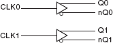
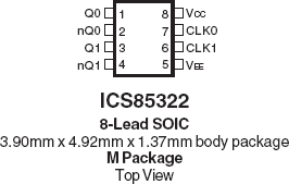
The 85322 is a Dual LVCMOS / LVTTL-to- Differential 2.5V / 3.3V LVPECL translator. The 85322 has selectable single ended clock inputs. The single ended clock input accepts LVCMOS or LVTTL input levels and translate them to 2.5V / 3.3V LVPECL levels. The small outline 8-pin SOIC package makes this device ideal for applications where space, high performance and low power are important.
Features
- Two differential 2.5V/3.3V LVPECL outputs
- Selectable CLK0, CLK1 LVCMOS/LVTTL clock inputs
- CLK0 and CLK1 can accepts the following input levels: LVCMOS or LVTTL
- Maximum output frequency: 267MHz
- Part-to-part skew: 250ps (maximum)
- 3.3V operating supply voltage (operating range 3.135V to 3.465V)
- 2.5V operating supply voltage (operating range 2.375V to 2.625V)
- 0°C to 70°C ambient operating temperature
- Lead-Free package available
Comparison
Applications
Design & Development
Models
ECAD Models
Schematic symbols, PCB footprints, and 3D CAD models from SamacSys can be found by clicking on products in the Product Options table. If a symbol or model isn't available, it can be requested directly from the website.

Processing table
| SOIC | 8 | C | Yes | Tube | ||
| SOIC | 8 | C | Yes | Reel |

Tips for Using This Parametric Table:
- Hide Filters button in header: Collapse or expands filters
- Column sort buttons in header: Sort Column alphabetically / numerically descending or ascending
- Reset button in header: Reset all filters to the page default
- Full Screen button in header: Expand the table to full screen view (user must close out of full screen before they can interact with rest of page)
- Export button in header: Export the filtered results of the table to an Excel document
- Filter parts search bar in header: Type to filter table results by part number
- Hide column button in column headers: Select to hide columns in table
- AND / OR toggle switches in header: Toggles the logic of this particular filter to be “AND” or “OR” logic for filtering results
- Multiselect checkboxes at beginning of each row in table: Select these checkboxes to compare products against each other
- Document icon next to product name in row: View the featured document for this product
- Chip icon next to the right of the document icon in row: View the block diagram for this product
- Cart icon to the right of the chip icon: Indicates that samples are available for this product