-
-
-
Design Resources
- Design & Development
- Featured Design Tools
- Partners
- Content & Training
-
Support
-
Support Forums
Get help from our expert Renesas technical staff and community.
- Technical Support
- Training & Events
- Quality & Packaging
-
Support Forums
-
Sample & Buy
-
Buy Direct from Renesas
Customers can now choose the convenience of buying direct from Renesas.
- Ordering Resources
-
Buy Direct from Renesas
SSTE32882KA1
circleObsoleteDDR3 Register + PLL
Jump to Page Section:
arrow_drop_down
Overview
Description
This 28-bit 1:2, or 26-bit 1:2 and 4-bit 1:1, registering clock driver with parity is designed for 1.25V, 1.35V and 1.5V VDD operation
Features
- DDR3-800/1066/1333/1600/1866/2133 rate
- 1-to-2 Register Outputs and 1-to-4 Clock Pair Outputs support stacked DDR3 RDIMMs
- Phase Lock Loop clock driver for buffering one differential clock pair (CK and CK) and distributing to four differential outputs
- Supports LVCMOS switching levels on the RESET and MIRROR inputs
- Checks priority on DIMM-independent data inputs
- Supports dynamic 1T/3T timing transaction and output inversion feature for improved timing performance during normal operations and MRS command pass-through
- Supports CKE Power Down operation modes
- Supports Quad Chip Select operation features
- RESET input disables differential input receivers, resets all registers, and disables all output drivers except ERROUT and QnCKEn
- Provides access to internal control words for configuring the device features and adapting in different RDIMM and system applications
- Latch-up performance exceeds 100mA
- ESD > 2000V per MIL-STD883, Method 3015; ESD > 200V using machine model (c = 200pF, R = 0)
Comparison
Applications
Documentation
= Featured Documentation
Log in required to subscribe
|
|
|
|
|---|---|---|
| Type | Title | Date |
| Datasheet | PDF 2.42 MB | |
| End Of Life Notice | PDF 1.11 MB | |
| Overview | PDF 515 KB | |
| Product Change Notice | PDF 27 KB | |
| Product Change Notice | PDF 33 KB | |
5 items
|
||
Design & Development
Models
ECAD Models
Schematic symbols, PCB footprints, and 3D CAD models from SamacSys can be found by clicking on products in the Product Options table. If a symbol or model isn't available, it can be requested directly from the website.

Product Options
Processing table
Pkg. Type |
Lead Count (#) |
Temp. Grade |
Pb (Lead) Free |
Carrier Type |
Buy / Sample |
|
|---|---|---|---|---|---|---|
| Part Number | ||||||
| CABGA | 176 | C | Yes | Tray | ||
| CABGA | 176 | C | Yes | Reel |

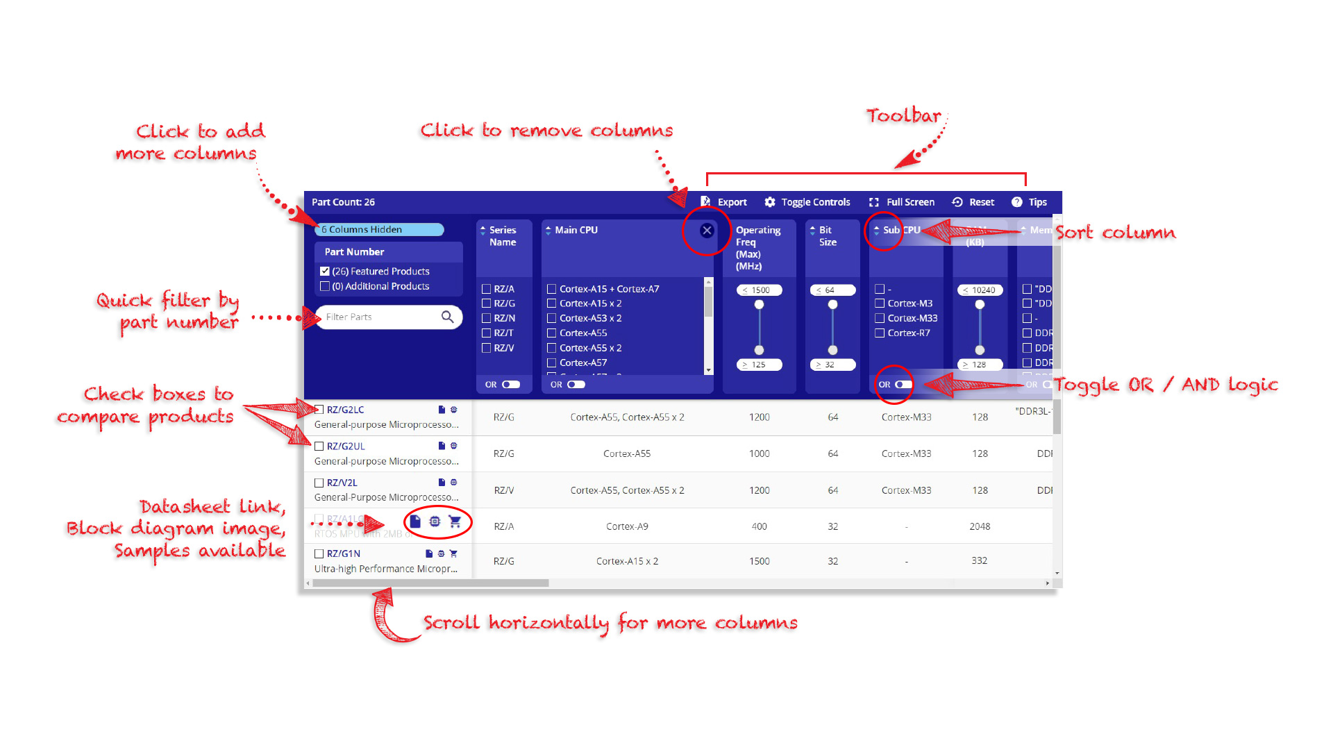
Tips for Using This Parametric Table:
- Hide Filters button in header: Collapse or expands filters
- Column sort buttons in header: Sort Column alphabetically / numerically descending or ascending
- Reset button in header: Reset all filters to the page default
- Full Screen button in header: Expand the table to full screen view (user must close out of full screen before they can interact with rest of page)
- Export button in header: Export the filtered results of the table to an Excel document
- Filter parts search bar in header: Type to filter table results by part number
- Hide column button in column headers: Select to hide columns in table
- AND / OR toggle switches in header: Toggles the logic of this particular filter to be “AND” or “OR” logic for filtering results
- Multiselect checkboxes at beginning of each row in table: Select these checkboxes to compare products against each other
- Document icon next to product name in row: View the featured document for this product
- Chip icon next to the right of the document icon in row: View the block diagram for this product
- Cart icon to the right of the chip icon: Indicates that samples are available for this product