
JESD204B/C Compliant Fanout Buffer and Divider
Jump to Page Section:
Overview
Description
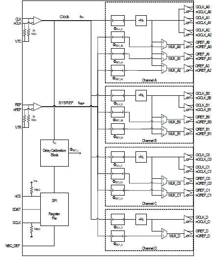
The 8V79S683 is a fully integrated, clock and SYSREF signal fanout buffer for JESD204B/C applications. It is designed as a high-performance clock and converter synchronization solution for wireless base station radio equipment boards with JESD204B/C subclass 0, 1, and 2 compliance. The main function of the device is the distribution and fanout of high-frequency clocks and low-frequency system reference signals generated by a JESB204B clock generator such as the IDT 8V19N490, extending its fanout capabilities and providing additional phase-delay. The 8V79S683 is optimized to deliver very low phase noise clocks and precise, phase-adjustable SYSREF synchronization signals. Low-skew outputs, low device-to-device skew characteristics and fast output rise/fall times help the system design to achieve deterministic clock and SYSREF phase relationship across devices.
The device distributes the input clock (CLK) and JESD204B SYSREF signals (REF) to four fanout channels. Input clock signals can be frequency divided and are fanned-out to multiple clock (QCLK_y) and SYSREF (QREF_r) outputs. Configurable phase-delay circuits are available for both clock and SYSREF signals. The propagation delays in all signal paths are fully deterministic to support fixed phase relationships between clock and SYSREF signals within one device. The device facilitates synchronization between frequency dividers within the device and across multiple devices, removing phase ambiguity introduced in dividers between power and configuration cycles.
Features
- Distribution, fanout, phase-delay of clock and SYSREF signals
- Very low output noise floor: -158.8dBc/Hz noise floor (245.76MHz)
- Supports clock frequencies up to 3GHz, including clock output frequencies of 983.04MHz, 491.52MHz, 245.76MHz, and 122.88MHz
- Four output channels with a total of 16 differential outputs
- Each channel contains frequency dividers and clock phase delay circuits
- Phase alignment mode across multiple buffers with any frequency divider setting
- Flexible differential outputs (LVDS/LVPECL/amplitude configurable)
- Configuration through 3-wire SPI interface
- Supply voltage:
- 3.3V core and signal I/O
- 1.8V Digital control SPI I/O (3.3V-tolerant inputs)
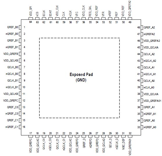
- 64-VFQFPN package (9 × 9 × 0.85 mm)
- Ambient temperature range: -40°C to +105°C (case)
Comparison
Applications
Documentation
= Featured Documentation
Log in required to subscribe
|
|
|
|
|---|---|---|
| Type | Title | Date |
| Datasheet | PDF 1.63 MB | |
| Product Change Notice | PDF 726 KB | |
| Overview | PDF 331 KB | |
3 items
|
||
Design & Development
Models
ECAD Models
Schematic symbols, PCB footprints, and 3D CAD models from SamacSys can be found by clicking on products in the Product Options table. If a symbol or model isn't available, it can be requested directly from the website.

Processing table
| VFQFPN | 64 | I | Yes | Tray | 3 | Get Samples, | ||
| VFQFPN | 64 | I | Yes | Reel | 3 | Get Samples, | ||
| VFQFPN | 64 | I | Yes | Reel | 3 | Get Samples, |

Tips for Using This Parametric Table:
- Hide Filters button in header: Collapse or expands filters
- Column sort buttons in header: Sort Column alphabetically / numerically descending or ascending
- Reset button in header: Reset all filters to the page default
- Full Screen button in header: Expand the table to full screen view (user must close out of full screen before they can interact with rest of page)
- Export button in header: Export the filtered results of the table to an Excel document
- Filter parts search bar in header: Type to filter table results by part number
- Hide column button in column headers: Select to hide columns in table
- AND / OR toggle switches in header: Toggles the logic of this particular filter to be “AND” or “OR” logic for filtering results
- Multiselect checkboxes at beginning of each row in table: Select these checkboxes to compare products against each other
- Document icon next to product name in row: View the featured document for this product
- Chip icon next to the right of the document icon in row: View the block diagram for this product
- Cart icon to the right of the chip icon: Indicates that samples are available for this product