Programmable Low Additive Jitter 2:8 Buffer with Dividers and Universal Outputs
Jump to Page Section:
Overview
Description
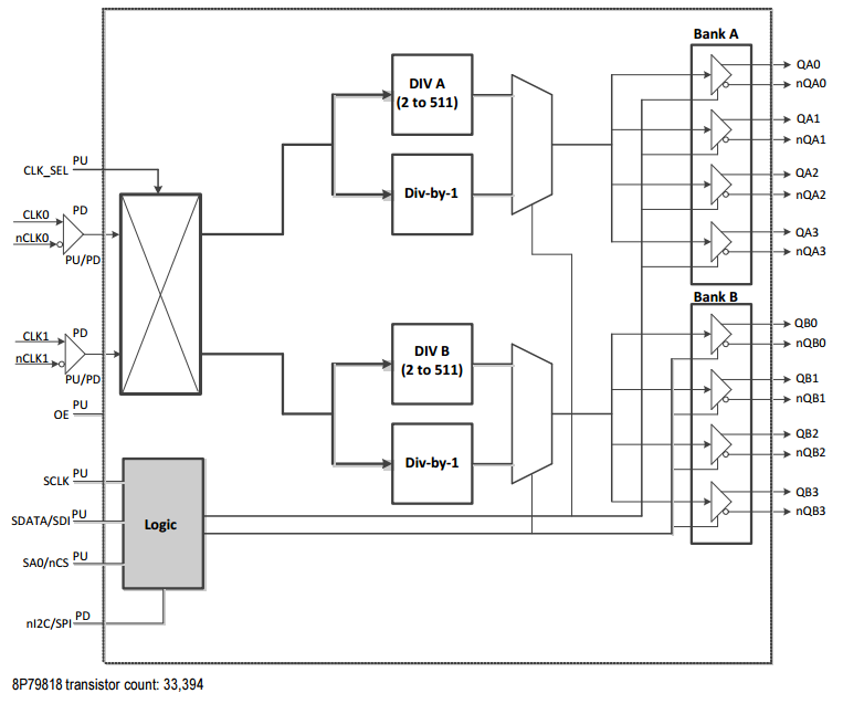
The device is intended to take 1 or 2 reference clocks, select between them, using a pin or register selection and generate up to 8 outputs that may be the same as the reference frequency or integer-divider versions of it.
The 8P79818 supports two output banks, each with its own divider and power supply. All outputs in one bank would generate the same output frequency, but each output can be individually controlled for output type, output enable or even powered-off.
The device supports a serial port for configuration of the parameters while in operation. The serial port can be selected to use the I2C or SPI protocol. After power-up, all outputs will come up in LVDS mode and may be programmed to other configurations over the serial port. Outputs may be enabled or disabled under control of the OE input pin.
The device can operate over the -40°C to +85°C temperature range.
Features
- Two differential inputs support LVPECL, LVDS, HCSL or LVCMOS reference clocks
- Select which of the two input clocks is to be used as the reference clock for which divider via pin or register selection
- Generates eight differential outputs or eight LVCMOS outputs, LVCMOS on Bank A only
- Outputs arranged in 2 banks of 4 outputs each
- Output enable control pin
- Register programmable via I2C / SPI serial port
- Core voltage supply of 3.3V, 2.5V or 1.8V
- -40°C to +85°C ambient operating temperature
- Lead-free (RoHS 6) packaging
Comparison
Applications
Design & Development
Models
ECAD Models
Schematic symbols, PCB footprints, and 3D CAD models from SamacSys can be found by clicking on products in the Product Options table. If a symbol or model isn't available, it can be requested directly from the website.

Processing table
| VFQFPN | 32 | I | Tray | 3 | 4.404 | Get Samples, | |
| VFQFPN | 32 | I | Reel | 3 | 4.404 | ||
| VFQFPN | 32 | I | Reel | 3 |

Tips for Using This Parametric Table:
- Hide Filters button in header: Collapse or expands filters
- Column sort buttons in header: Sort Column alphabetically / numerically descending or ascending
- Reset button in header: Reset all filters to the page default
- Full Screen button in header: Expand the table to full screen view (user must close out of full screen before they can interact with rest of page)
- Export button in header: Export the filtered results of the table to an Excel document
- Filter parts search bar in header: Type to filter table results by part number
- Hide column button in column headers: Select to hide columns in table
- AND / OR toggle switches in header: Toggles the logic of this particular filter to be “AND” or “OR” logic for filtering results
- Multiselect checkboxes at beginning of each row in table: Select these checkboxes to compare products against each other
- Document icon next to product name in row: View the featured document for this product
- Chip icon next to the right of the document icon in row: View the block diagram for this product
- Cart icon to the right of the chip icon: Indicates that samples are available for this product
Videos & Training
News & Blog Posts
| Blog Post | Dec 15, 2018 |