Low Additive Jitter 2:8 Buffer with CMOS / Differential Outputs
Jump to Page Section:
Overview
Description
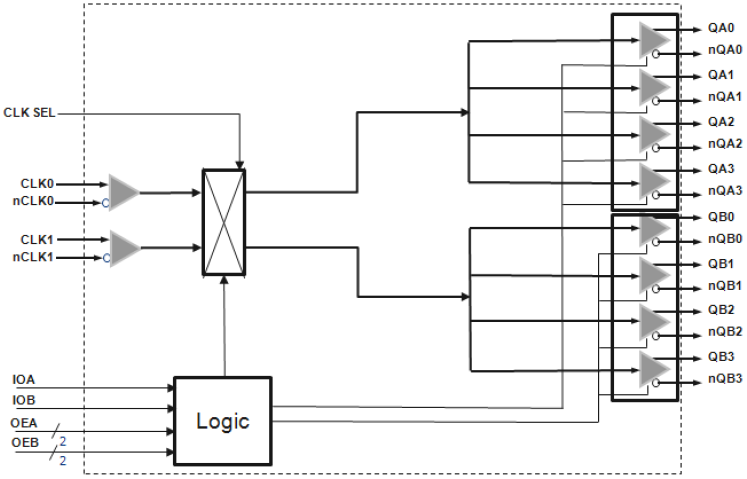
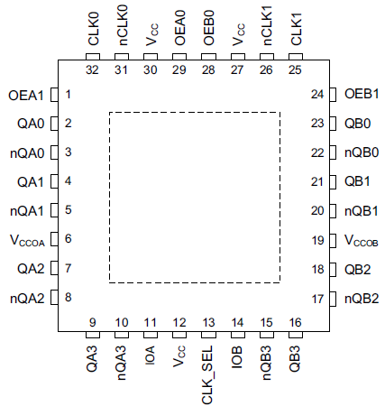
The 8P791208 is a low additive jitter 2:8 buffer with CMOS / differential outputs. The device takes 1 or 2 reference clocks, selects between them, using a pin selection and generates up to 8 outputs that are the same as the reference frequency. The 8P791208 supports two output banks, each with its own power supply. All outputs in one bank generate the same output frequency, but each output can be individually controlled for output type or output enable. The device can operate over the -40°C to 85°C temperature range.
Features
- Accepts input frequencies ranging from 1PPS (1Hz) to 700MHz
- Two differential inputs support LVPECL, LVDS, LVHSTL, HCSL or LVCMOS reference clocks
- Generates 8 differential or 16 LVCMOS outputs
- Outputs arranged in two banks of four outputs each
- Select pins control which input drives which of two output banks
- Controlled by 3-level input pins that are 3.3V-tolerant for all core voltages
- Output type may be selected from LVPECL, LVDS or 2xLVCMOS
- Each bank supports a separate power supply of 3.3V, 2.5V or
- LVCMOS outputs are limited to 125MHz maximum and support swings of 3.3V, 2.5V, 1.8V and 1.5V
- Individual output enables and output type selection supported
- Output noise floor of –158dBc/Hz @ 156.25MHz
- Core voltage supply of 3.3V, 2.5V or 1.8V
- -40°C to +85°C ambient operating temperature
- Lead-free (RoHS 6) QFN-32 (5 × 5 mm) packaging
Comparison
Applications
Design & Development
Models
ECAD Models
Schematic symbols, PCB footprints, and 3D CAD models from SamacSys can be found by clicking on products in the Product Options table. If a symbol or model isn't available, it can be requested directly from the website.

Processing table
| VFQFPN | 32 | I | Tray | 3 | Get Samples, | ||
| VFQFPN | 32 | I | Reel | 3 | 6.985 | ||
| VFQFPN | 32 | I | Reel | 3 |

Tips for Using This Parametric Table:
- Hide Filters button in header: Collapse or expands filters
- Column sort buttons in header: Sort Column alphabetically / numerically descending or ascending
- Reset button in header: Reset all filters to the page default
- Full Screen button in header: Expand the table to full screen view (user must close out of full screen before they can interact with rest of page)
- Export button in header: Export the filtered results of the table to an Excel document
- Filter parts search bar in header: Type to filter table results by part number
- Hide column button in column headers: Select to hide columns in table
- AND / OR toggle switches in header: Toggles the logic of this particular filter to be “AND” or “OR” logic for filtering results
- Multiselect checkboxes at beginning of each row in table: Select these checkboxes to compare products against each other
- Document icon next to product name in row: View the featured document for this product
- Chip icon next to the right of the document icon in row: View the block diagram for this product
- Cart icon to the right of the chip icon: Indicates that samples are available for this product
Videos & Training
News & Blog Posts
| Blog Post | Dec 15, 2018 |