
1:12, LVDS Output Fanout Buffer
Jump to Page Section:
Overview
Description
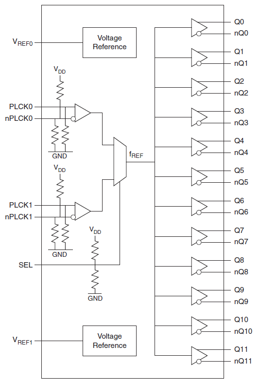
The 8SLVD1212 is a high-performance differential LVDS fanout buffer. The device is designed for the fanout of high-frequency, very low additive phase-noise clock and data signals. The 8SLVD1212 is characterized to operate from a 2.5V power supply. Guaranteed output-to-output and part-to-part skew characteristics make the 8SLVD1212 ideal for those clock distribution applications demanding well-defined performance and repeatability. Two selectable differential inputs and twelve low skew outputs are available. The integrated bias voltage reference enables easy interfacing of single-ended signals to the device inputs. The device is optimized for low power consumption and low additive phase noise.
Features
- Twelve low skew, low additive jitter LVDS output pairs
- Two selectable, differential clock input pairs
- Differential PCLK, nPCLK pairs can accept the following differential
input levels: LVDS, LVPECL, CML - Maximum input clock frequency: 2GHz (maximum)
- LVCMOS/LVTTL interface levels for the control input select pins
- Output skew: 40ps (max)
- Propagation delay: 310ps (typical)
- Low additive phase jitter, RMS; fREF = 156.25MHz,
10kHz - 20MHz: 77fs (typical) - Maximum device current consumption (IDD): 213mA
- 2.5V supply voltage
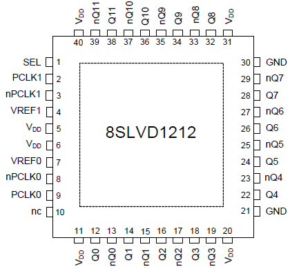
- Lead-free (RoHS 6), 40-Lead VFQFN packaging
- -40°C to 85°C ambient operating temperature
Comparison
Applications
Design & Development
Models
ECAD Models
Schematic symbols, PCB footprints, and 3D CAD models from SamacSys can be found by clicking on products in the Product Options table. If a symbol or model isn't available, it can be requested directly from the website.

Processing table
| VFQFPN | 40 | I | Yes | Tray | 3 | Get Samples, | ||
| VFQFPN | 40 | I | Yes | Reel | 3 | |||
| VFQFPN | 40 | I | Yes | Reel | 3 |

Tips for Using This Parametric Table:
- Hide Filters button in header: Collapse or expands filters
- Column sort buttons in header: Sort Column alphabetically / numerically descending or ascending
- Reset button in header: Reset all filters to the page default
- Full Screen button in header: Expand the table to full screen view (user must close out of full screen before they can interact with rest of page)
- Export button in header: Export the filtered results of the table to an Excel document
- Filter parts search bar in header: Type to filter table results by part number
- Hide column button in column headers: Select to hide columns in table
- AND / OR toggle switches in header: Toggles the logic of this particular filter to be “AND” or “OR” logic for filtering results
- Multiselect checkboxes at beginning of each row in table: Select these checkboxes to compare products against each other
- Document icon next to product name in row: View the featured document for this product
- Chip icon next to the right of the document icon in row: View the block diagram for this product
- Cart icon to the right of the chip icon: Indicates that samples are available for this product