High Speed A/D Converter Evaluation Kits
Renesas offers two options for evaluating high-speed analog-to-digital converter products with LVDS and/or LVCMOS outputs. A complete, turnkey evaluation platform is...

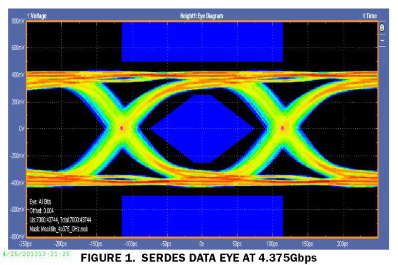
The ISLA214S50 is a series of low-power, high-performance, 14-bit, analog-to-digital converters. Designed with FemtoCharge™ technology on a standard CMOS process, the series supports sampling rates of up to 500MSPS. The ISLA214S50 is part of a pin-compatible family of 12-, 14-, and 16-bit A/Ds with maximum sample rates ranging from 125MSPS to 500MSPS. The family minimizes power consumption while providing state-of-the-art dynamic performance. The device utilizes two time-interleaved 250MSPS unit ADCs to achieve the ultimate sample rate of 500MSPS. A single 500MHz conversion clock is presented to the converter, and all interleave clocking is managed internally. The proprietary Intersil Interleave Engine (I2E) performs automatic correction of offset, gain, and sample time mismatches between the unit ADCs to optimize performance. The ISLA214S50 offers a highly configurable, JESD204Bcompliant, high speed serial output link. The link offers data rates up to 4. 375 Gbps per lane and multiple packing modes. The link can be configured to use two or three lanes to transmit the conversion data, allowing for flexibility in the receiver design. The JESD204 transmitter also provides deterministic latency and multi-chip time alignment support to satisfy complex synchronization requirements. A serial peripheral interface (SPI) port allows for extensive configurability of the ADC and its JESD204B transmitter including access to its built-in link and transport-layer test patterns as well as the programmable clock divider, enabling 2x harmonic clocking. The ISLA214S50 is available in a space-saving 7mmx7mm 48 Ld QFN package. The package features a thermal pad for improved thermal performance and is specified over the full industrial temperature range (-40°C to +85°C)
|
|
|
|
|---|---|---|
| 类型 | 文档标题 | 日期 |
| 数据手册 | PDF 2.15 MB | |
| End Of Life Notice | PDF 1.17 MB | |
| 指南 | PDF 715 KB | |
| 手册 - 开发工具 | PDF 503 KB | |
| 应用文档 | PDF 503 KB | |
| 应用文档 | PDF 1.08 MB | |
| 应用文档 | PDF 287 KB | |
7 items
|
||
Renesas offers two options for evaluating high-speed analog-to-digital converter products with LVDS and/or LVCMOS outputs. A complete, turnkey evaluation platform is...
Renesas offers a complete, turnkey evaluation platform that includes data capture hardware and software to process and display acquired data. This system provides the...
Schematic symbols, PCB footprints, and 3D CAD models from SamacSys can be found by clicking on products in the Product Options table. If a symbol or model isn't available, it can be requested directly from the website.

| QFN | Tray |