画像


Renesasの低ジッターなクロックジェネレータは、すべてPLLをベースとしています。アプリケーションにおける必要に応じ、複数のクロック信号を生成することが可能です。この製品カテゴリには、ほとんどのシリアル・データ・アプリケーションに適した低位相ノイズの発振器が含まれています。また各クロック・ジェネレータは、シングルエンド/差動のさまざまな信号形式(LVCMOS、LVPEC、LVDS、HCSL、SSTL、HSTLなど)に対応します。
Renesasのクロック・ジェネレータでは、位相ノイズの少ないファンアウト・バッファを使用して、複数の信号を複製したり、異なる形式の出力を追加したりすることができます。Renesasは、低ジッターのクロック・ジェネレータや低位相ノイズの発振器を業界で最も多く取りそろえています。そのため、高度に最適化を図ったソリューションを構築することが可能です。PCI Express、RF、ネットワーク同期など、特定アプリケーションに向けた低ジッターのクロック。
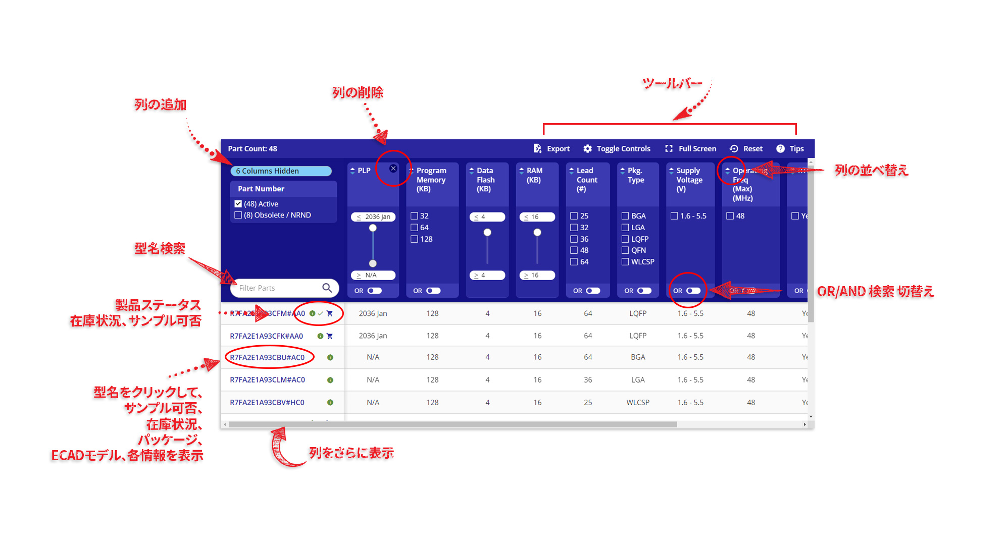
ヒント:100MHzと125MHzといった具合に、複数の特定出力周波数が必要な場合には、パラメトリック検索において「Output Banks(出力バンク)」を活用してください。各バンクは、特定の出力周波数に対応しています。なお、出力数はデバイスによって大きく異なります。
特定アプリケーションに向けた低ジッターのクロックジェネレータを選定する際には、いくつかの重要な事柄について検討する必要があります。以下に示すパラメータについて検討することで、ソリューションを構築する際の出発点となる基本的な情報を得ることができます。
低ジッターのクロックジェネレータ(低位相ノイズの発振器)について
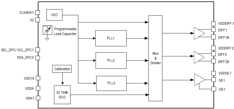
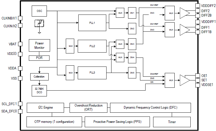
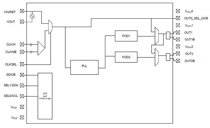
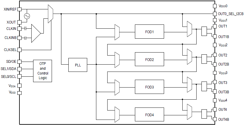
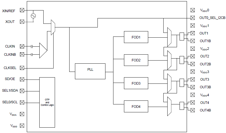
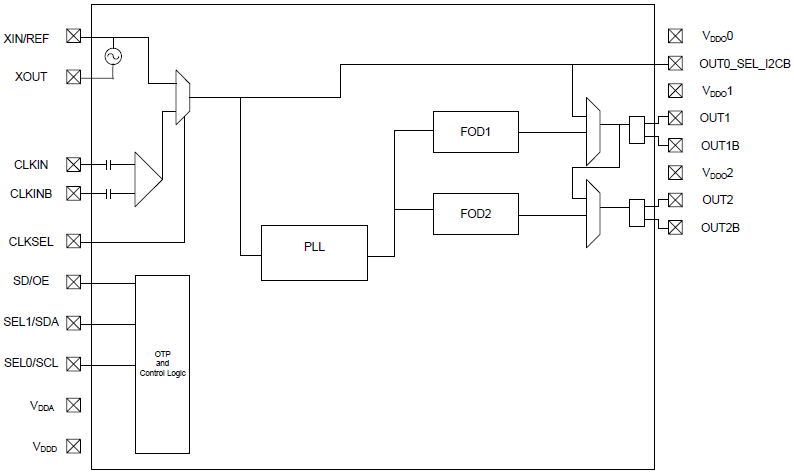
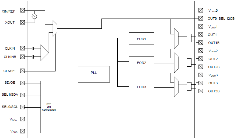
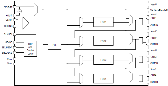
低ジッターのクロックジェネレータは、システムの同期動作を実現するためのタイミング信号を生成する高度なICです。最も基本的なレベルで表現すれば、共振回路とアンプで構成されるものだと言うことができます。得られるタイミング信号としては、デューティ・サイクルが50%の単純な方形波はもちろん、それ以外のアレンジを加えることも可能です。この場合の共振回路は、一般に、圧電水晶振動子を使用する低位相ノイズの発振回路です。Renesasは、低位相ノイズの発振器を必要とするあらゆるアプリケーションに対応できるよう、消費電力、性能、柔軟性の面でバリエーションを持った低ジッターのクロック製品ファミリをいくつか提供しています。
Outputs (#) |
Output Type |
Output Freq Range (MHz) |
Input Freq (MHz) |
Inputs (#) |
Input Type |
Output Banks (#) |
Core Voltage (V) |
Output Voltage (V) |
Phase Jitter Typ RMS (ps) |
Phase Jitter Max RMS (ps) |
105°C Max. Case Temp. |
|
|---|---|---|---|---|---|---|---|---|---|---|---|---|
| 型名 | ||||||||||||
| VersaClock® 3S Programmable Clock Generator | 5 | LP-HCSL, LVCMOS | 0.032768 - 125 | 1 - 160 | 1 | Crystal, HCSL, LVCMOS, LVDS, LVPECL | 3 | 1.8 | 1.8 | 3 | ||
| VersaClock® 3Sプログラマブルクロックジェネレータ | 5 | LP-HCSL, LVCMOS, LVDS, LVPECL | 0.032768 - 500 | 1 - 160 | 1 | Crystal, LP-HCSL, LVCMOS, LVDS, LVPECL | 3 | 3.3 | 1.8, 2.5, 3.3 | 3 | ||
| VersaClock® 5 Low Power Programmable Clock Generator | 3 | HCSL, LVCMOS, LVDS, LVPECL | 1 - 350 | 1 - 350 | 2 | Crystal, HCSL, LVCMOS, LVDS, LVPECL | 2 | 1.8, 2.5, 3.3 | 1.8, 2.5, 3.3 | 0.7 | 1.5 | |
| VersaClock® 6E プログラマブルクロックジェネレータ | 5 | HCSL, LVCMOS, LVDS, LVPECL | 1 - 350 | 1 - 350 | 2 | Crystal, HCSL, LVCMOS, LVDS, LVPECL | 4 | 1.8, 2.5, 3.3 | 1.8, 2.5, 3.3 | 0.5 | ||
| VersaClock® 6 Low Power Programmable Clock Generator | 5 | HCSL, LVCMOS, LVDS, LVPECL | 1 - 350 | 1 - 350 | 2 | Crystal, HCSL, LVCMOS, LVDS, LVPECL | 4 | 1.8, 2.5, 3.3 | 1.8, 2.5, 3.3 | 0.5 | ||
| VersaClock® 6 Low Power Programmable Clock Generator | 3 | HCSL, LVCMOS, LVDS, LVPECL | 1 - 350 | 1 - 350 | 2 | Crystal, HCSL, LVCMOS, LVDS, LVPECL | 2 | 1.8, 2.5, 3.3 | 1.8, 2.5, 3.3 | 0.5 | ||
| VersaClock® 6 Low Power Programmable Clock Generator | 4 | HCSL, LVCMOS, LVDS, LVPECL | 1 - 350 | 1 - 350 | 2 | Crystal, HCSL, LVCMOS, LVDS, LVPECL | 3 | 1.8, 2.5, 3.3 | 1.8, 2.5, 3.3 | 0.5 | ||
| VersaClock® 6Eプログラマブルクロックジェネレータ | 5 | HCSL, LVCMOS, LVDS, LVPECL | 1 - 350 | 1 - 350 | 2 | Crystal, HCSL, LVCMOS, LVDS, LVPECL | 4 | 1.8, 2.5, 3.3 | 1.8, 2.5, 3.3 | 0.5 | ||
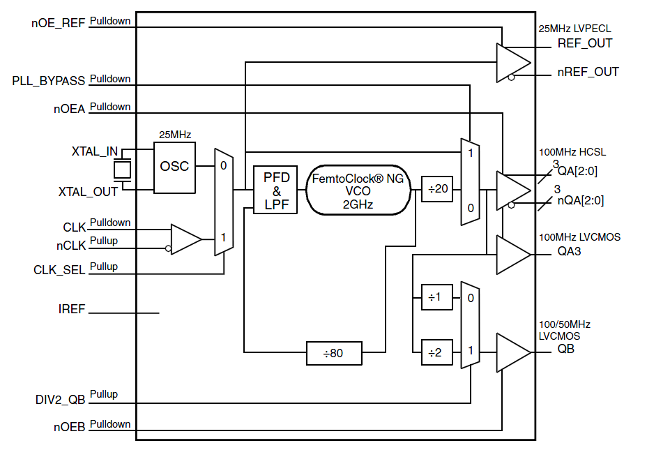
| FemtoClock™ NG Crystal-To-HCSL Frequency Synthesizer | 6 | HCSL, LVCMOS, LVPECL | 25 - 100 | 25 | 2 | Crystal, HCSL, LVDS, LVPECL | 4 | 3.3 | 3.3 | 0.34 | ||
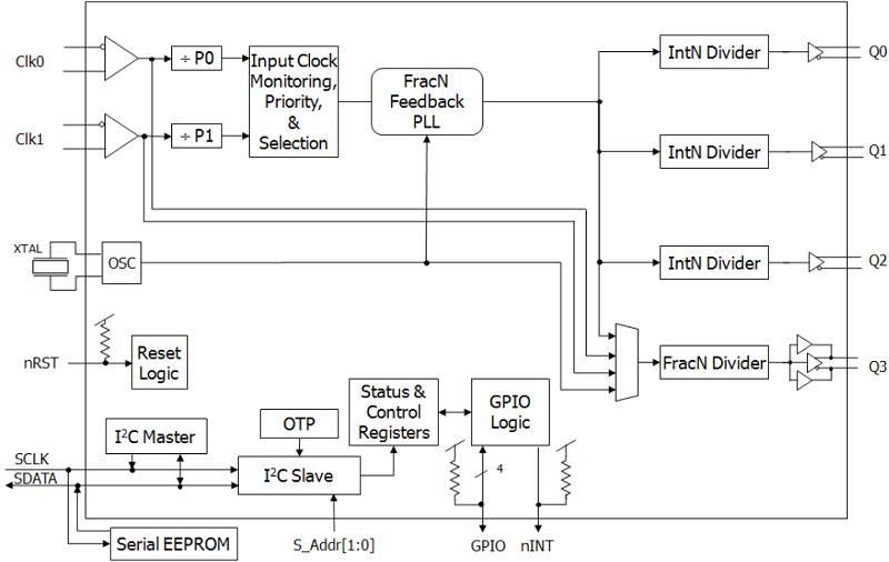
| FemtoClock™ NGユニバーサル周波数トランスレータ | 4 | HCSL, LVCMOS, LVDS, LVPECL | 0.008 - 1000 | 0.008 - 875 | 2 | HCSL, LVCMOS, LVDS, LVHSTL, LVPECL, LVTTL | 4 | 2.5, 3.3 | 1.8, 2.5, 3.3 | 0.2 | ||
| FemtoClock™ NGユニバーサル周波数トランスレータ | 4 | HCSL, LVCMOS, LVDS, LVPECL | 0.008 - 1000 | 0.008 - 875 | 2 | HCSL, LVCMOS, LVDS, LVHSTL, LVPECL, LVTTL | 4 | 2.5, 3.3 | 1.8, 2.5, 3.3 | 0.35 | ||
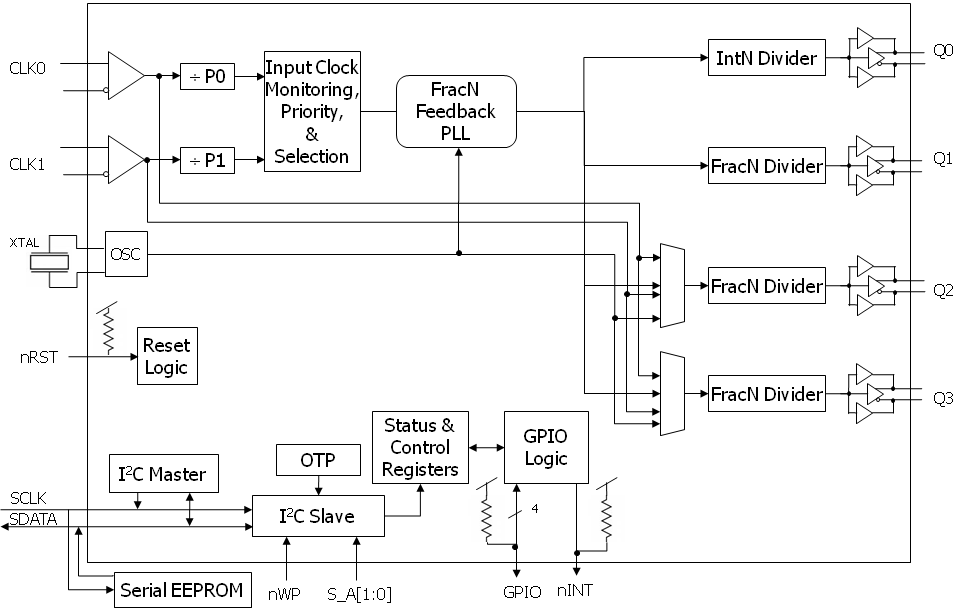
| FemtoClock NG Triple Universal Frequency Translator | 6 | LVDS, LVPECL | 0.98 - 1300 | 0.008 - 710 | 7 | HCSL, LVCMOS, LVDS, LVHSTL, LVPECL, LVTTL | 3 | 2.5 | 2.5 | 0.333 | 0.465 |
Description:
Lab demonstration and clock jitter measurement showing VersaClock 5. The frequency analyzer shows phase jitter at approximately 575 picoseconds RMS. Presented by Baljit Chandhoke, product manager at IDT. For more information visit the Programmable Clocks page.
Transcript:
Hello, my name is Baljit Chandhoke, and I'm the Product Line Manager of timing products at IDT. Today, I will be giving you a brief lab demonstration of our new product, "VersaClock 5".
VersaClock 5 is a low power clock generator, with best-in-class jitter performance of 0.7 psec. It has extremely low power with core current consumption of only 30 MA. It is extremely programmable, and you can get any frequency you want at the output, up to 350MHz.
Now I'm going to start the lab demonstration. I have with me, an evaluation board. The evaluation board is powered by the USB cable, and is also used to control the VersaClock 5.
This is the Timing Commander software, which controls the VersaClock 5 device. As you see, I have it configured for 125MHz, LVPECL output, on Output 1.
On Output 2, I have it configured at 125MHz, HCSL output. Output 3, I have it configured at 156.25MHz LVDS, and Output 4 has 312.5MHz. All the outputs are operational and have different output frequencies.
Now, let's take a look at the performance. With all these outputs operational, and on Output 1, which is operating at 125MHz, I see 575 fsec RMS phase jitter from 12K to 20MHz.
This is industry leading in the power consumption of 30MA core in the space.
Now let's change the frequency and see what happens to the phase noise. I'm going to change the frequency on Output 1 to 100MHz.
As you see, the frequency changed to 100MHz as shown on the screen, and the phase noise is still 576 fsec, from 12K to 20MHz. The noise floor is close to 150dBc.
So this product maintains the great performance, across a wide range of frequencies, as well as across multiple output types, and with different frequencies of the output.
So it provides you, a complete system solution, meeting the requirements of all your clocking needs in your system.
