
概要
説明
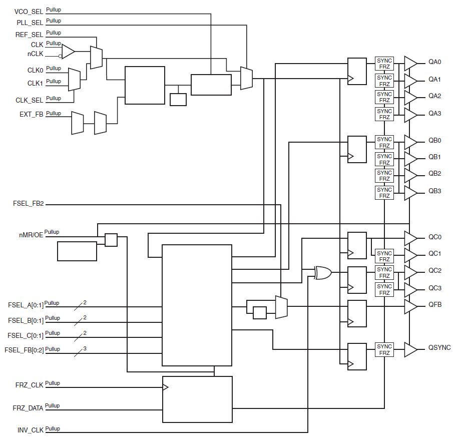
The 87973I is a LVCMOS/LVTTL clock generator from IDT. The 87973I has three selectable inputs and provides fourteen LVCMOS/LVTTL outputs. The 87973I is a highly flexible device. The three selectable inputs (1 differential and 2 single ended inputs) are often used in systems requiring redundant clock sources. Up to three different output frequencies can be generated among the three output banks. The three output banks and feedback output each have their own output dividers which allows the device to generate a multitude of different bank frequency ratios and output-to-input frequency ratios. In addition, 2 outputs in Bank C (QC2, QC3) can be selected to be inverting or non-inverting. The output frequency range is 8.33MHz to125MHz. The input frequency range is 5MHz to 120MHz. The 87973I also has a QSYNC output which can by used for system synchronization purposes. It monitors Bank A and Bank C outputs and goes low one period prior to coincident rising edges of Bank A and Bank C clocks. QSYNC then goes high again when the coincident rising edges of Bank A and Bank C occur. This feature is used primarily in applications where Bank A and Bank C are running at different frequencies, and is particularly useful when they are running at non-integer multiples of one another.
特長
- Fully integrated PLL
- Fourteen LVCMOS/LVTTL outputs
- twelve clock outputs, one feedback, one sync
- Selectable LVCMOS/LVTTL or differential CLK, nCLK inputs
- CLK0, CLK1 can accept the following input levels: LVCMOS or LVTTL
- CLK, nCLK pair can accept the following differential input levels: LVPECL, LVDS, LVHSTL, SSTL, HCSL
- Output frequency range: 8.33MHz to 125MHz
- VCO range: 200MHz to 480MHz
- Output skew: 550ps (maximum)
- Cycle-to-cycle jitter: ±100ps (typical)
- Full 3.3V supply voltage
- -40°C to 85°C ambient operating temperature
- Available in lead-free RoHS compliant package
- Compatible with PowerPC™ and Pentium™ Microprocessors
製品比較
アプリケーション
ドキュメント
= ピックアップ
ログイン後、ご登録が可能となります。
|
|
|
|
|---|---|---|
| 分類 | タイトル | 日時 |
| データシート | PDF 325 KB | |
| EOL通知 | PDF 743 KB | |
| EOL通知 | PDF 715 KB | |
| EOL通知 | PDF 218 KB | |
| 製品変更通知 | PDF 36 KB | |
5 items
|
||
設計・開発
モデル
ECADモデル
[製品選択]テーブル内の製品名をクリックするとSamacSysが提供する回路図シンボル、PCBフットプリント、3D CADモデルがご確認いただけます。 お探しのシンボルやモデルが見つからない場合、Webサイトから直接リクエストできます。

Processing table
| TQFP | 52 | I | Yes | Tray | ||
| TQFP | 52 | I | Yes | Reel |

Tips for Using This Parametric Table:
- Hide Filters button in header: Collapse or expands filters
- Column sort buttons in header: Sort Column alphabetically / numerically descending or ascending
- Reset button in header: Reset all filters to the page default
- Full Screen button in header: Expand the table to full screen view (user must close out of full screen before they can interact with rest of page)
- Export button in header: Export the filtered results of the table to an Excel document
- Filter parts search bar in header: Type to filter table results by part number
- Hide column button in column headers: Select to hide columns in table
- AND / OR toggle switches in header: Toggles the logic of this particular filter to be “AND” or “OR” logic for filtering results
- Multiselect checkboxes at beginning of each row in table: Select these checkboxes to compare products against each other
- Document icon next to product name in row: View the featured document for this product
- Chip icon next to the right of the document icon in row: View the block diagram for this product
- Cart icon to the right of the chip icon: Indicates that samples are available for this product