
1:4, Differential-to-LVCMOS / LVTTL Zero Delay Clock Generator
ページセクションへ移動:
概要
説明
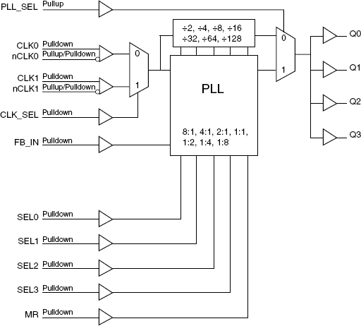
The 87004I is a highly versatile 1:4 Differential-to-LVCMOS/LVTTL Clock Generator. The 87004I has two selectable clock inputs. The CLK0, nCLK0 and CLK1, nCLK1 pairs can accept most standard differential input levels. Internal bias on the nCLK0 and nCLK1 inputs allows the CLK0 and CLK1 inputs to accept LVCMOS / LVTTL. The 87004I has a fully integrated PLL and can be configured as a zero delay buffer, multiplier or divider and has an input and output frequency range of 15.625 MHz to 250 MHz. The reference divider, feedback divider and output divider are each programmable, thereby allowing for the following output-to-input frequency ratios: 8:1, 4:1, 2:1, 1:1, 1:2, 1:4, 1:8. The external feedback allows the device to achieve "zero delay" between the input clock and the output clocks. The PLL_SEL pin can be used to bypass the PLL for system test and debug purposes. In bypass mode, the reference clock is routed around the PLL and into the internal output dividers.
特長
- Four LVCMOS / LVTTL outputs, 7Ω typical output impedance
- Selectable CLK0/nCLK0 or CLK1/nCLK1 clock inputs
- CLKx/nCLKx pairs can accept the following differential input levels: LVPECL, LVDS, LVHSTL, HCSL, SSTL
- Internal bias on nCLK0 and nCLK1 to support LVCMOS / LVTTL levels on CLK0 and CLK1 inputs
- Output frequency range: 15.625 MHz to 250 MHz
- Input frequency range: 15.625 MHz to 250 MHz
- VCO range: 250 MHz to 500 MHz
- External feedback for "zero delay" clock regeneration with configurable frequencies
- Programmable dividers allow for the following output-to-input frequency ratios: 8:1, 4:1, 2:1, 1:1, 1:2, 1:4, 1:8
- Fully integrated PLL
- Cycle-to-cycle jitter: 45 ps (maximum)
- Output skew: 65 ps (maximum)
- Static phase offset: 50 ps ±150 ps (3.3 V ±5%), CLK0/nCLK0
- Full 3.3 V or 2.5 V output operating supply
- 5 V tolerant
- -40°C to 85°C ambient operating temperature
- Available in both standard (RoHS 5) and lead-free (RoHS 6) packages
製品比較
アプリケーション
設計・開発
モデル
ECADモデル
[製品選択]テーブル内の製品名をクリックするとSamacSysが提供する回路図シンボル、PCBフットプリント、3D CADモデルがご確認いただけます。 お探しのシンボルやモデルが見つからない場合、Webサイトから直接リクエストできます。

Processing table
| TSSOP | 24 | I | Yes | Tube | ||
| TSSOP | 24 | I | Yes | Reel |

Tips for Using This Parametric Table:
- Hide Filters button in header: Collapse or expands filters
- Column sort buttons in header: Sort Column alphabetically / numerically descending or ascending
- Reset button in header: Reset all filters to the page default
- Full Screen button in header: Expand the table to full screen view (user must close out of full screen before they can interact with rest of page)
- Export button in header: Export the filtered results of the table to an Excel document
- Filter parts search bar in header: Type to filter table results by part number
- Hide column button in column headers: Select to hide columns in table
- AND / OR toggle switches in header: Toggles the logic of this particular filter to be “AND” or “OR” logic for filtering results
- Multiselect checkboxes at beginning of each row in table: Select these checkboxes to compare products against each other
- Document icon next to product name in row: View the featured document for this product
- Chip icon next to the right of the document icon in row: View the block diagram for this product
- Cart icon to the right of the chip icon: Indicates that samples are available for this product