
Dual Synchronous Ethernet Line Card PLL
Jump to Page Section:
Overview
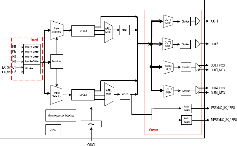
Description
The 82V3395 is an integrated, single-chip solution for the Synchronous Equipment Timing applications in SONET / SDH / Synchronous Ethernet equipment, DWDM and Wireless base station. The device supports several types of input clock sources: recovered clock from Synchronous Ethernet, STM-N or OC-n, PDH network synchronization timing and external synchronization reference timing. The device consists of 2 DPLL+APLL paths. The two path lock independently from each other. An input clock is automatically or manually selected for both path. Both paths support three primary operating modes: Free-Run, Locked and Holdover. In Free-Run mode, the DPLL refers to the master clock. In Locked mode, the DPLL locks to the selected input clock. In Holdover mode, the DPLL resorts to the frequency data acquired in Locked mode. Whatever the operating mode is, the DPLL gives a stable performance without being affected by operating conditions or silicon process variations. There are 2 high performance APLLs that can be used for low jitter SONET and Ethernet Clocks The device provides programmable DPLL bandwidths: 18 Hz, 35 Hz, 70 Hz and 560 Hz. A stable input is required for the master clock in different applications. The master clock is used as a reference clock for all the internal circuits in the device. All the read/write registers are accessed through a microprocessor interface. The device supports I2C and serial microprocessor interface modes.
Features
- Provides node clock for ITU-T G.8261/G.8262 Synchronous Ethernet (SyncE)
- Exceeds GR-253-CORE (OC-12) and ITU-T G.813 (STM-4) jitter generation requirements
- Provides node clocks for Cellular and WLL base-station (GSM and 3G networks)
- Provides clocks for 1 Gigabit and 10 Gigabit Ethernet applications
- Employs PLL architecture to feature excellent jitter performance and minimize the number of external components
- Integrates 2 DPLLs
- one can be used on the transmit path and the other on the receive path
- Supports programmable DPLL bandwidth: 18 Hz, 35 Hz, 70 Hz and 560 Hz
- Provides OUT1~OUT4 output clock frequencies up to 644.53125 MHz
- Includes 25MHz, 125 MHz and 156.25 MHz for CMOS outputs
- Includes 25.78125MHz, 128.90625 MHz and 161.1328125 MHz for CMOS outputs
- Includes 25MHz, 125 MHz, 156.25 MHz, 312.5 MHz and 625 MHz for differential outputs
- Includes 25.78125 MHz, 128.90625 MHz, 161.1328125 MHz, 322.265625 MHz and 644.53125 MHz for differential outputs
- Provides IN1~IN4 input clock frequencies cover from 2 kHz to 155.52MHz MHz
- Supports Forced or Automatic operating mode switch controlled by an internal state machine. It supports Free- Run, Locked and Holdover modes
- Supports manual and automatic selected input clock switch
- Supports automatic hitless selected input clock switch on clock failure
- Supports three types of input clock sources: recovered clock from STM-N or OC-n, PDH network synchronization timing and external synchronization reference timing
- Provides a 2 kHz, 4 kHz, or 8 kHz frame sync input signal, and a 2 kHz or 8 kHz frame sync output signals
- Provides a 1PPS sync input signal and a 1PPS sync output signal
- Provides output clocks for BITS, GPS, 3G, GSM, etc.
- Supports PECL/LVDS and CMOS input/output technologies
- Supports master clock calibration
- Supports Telcordia GR-1244-CORE, Telcordia GR-253-CORE, ITU-T G.812, ITU-T G.8262. ITU-T G.813 and ITU-T G.783 Recommendations
- I2C and Serial microprocessor interface modes
- IEEE 1149.1 JTAG Boundary Scan
- Single 3.3 V operation with 5 V tolerant CMOS I/Os
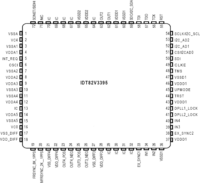
- 72-pin QFN package, green package options available
Comparison
Applications
Design & Development
Models
ECAD Models
Schematic symbols, PCB footprints, and 3D CAD models from SamacSys can be found by clicking on products in the Product Options table. If a symbol or model isn't available, it can be requested directly from the website.

Processing table
| VFQFPN | 72 | C | Yes | Tray | 40.81 | Get Samples, | |
| VFQFPN | 72 | C | Yes | Reel |

Tips for Using This Parametric Table:
- Hide Filters button in header: Collapse or expands filters
- Column sort buttons in header: Sort Column alphabetically / numerically descending or ascending
- Reset button in header: Reset all filters to the page default
- Full Screen button in header: Expand the table to full screen view (user must close out of full screen before they can interact with rest of page)
- Export button in header: Export the filtered results of the table to an Excel document
- Filter parts search bar in header: Type to filter table results by part number
- Hide column button in column headers: Select to hide columns in table
- AND / OR toggle switches in header: Toggles the logic of this particular filter to be “AND” or “OR” logic for filtering results
- Multiselect checkboxes at beginning of each row in table: Select these checkboxes to compare products against each other
- Document icon next to product name in row: View the featured document for this product
- Chip icon next to the right of the document icon in row: View the block diagram for this product
- Cart icon to the right of the chip icon: Indicates that samples are available for this product