-
-
设计资源
- 设计和开发
- 特色设计工具
- 合作伙伴
- 内容和培训
概览
简介
The evaluation kit supports the electrical evaluation process of the 8V19N882NVGI JESD204B/C clock jitter attenuator for all major device parameters including phase noise, spurious attenuation, clock frequency, output skew, phase alignment, device timing and the signal waveform. The device is a central source of phase-aligned clock and SYSREF signals in JESD204B/C applications. Its two stage PLL architecture is optimized for jitter attenuation and low phase noise, high frequency clock generation. The first stage PLL use an external VCXO component located on the evaluation board, the second stage uses an internal VCO or optionally, an external VCO. The internal VCO has a center frequency of 3.93216 GHz allowing the generation of wireless infrastructure reference frequencies. The optional external VCO component, when populated and selected, can be anywhere in the range of 700 MHz to 6 GHz supporting arbitrary frequency plans. The evaluation board has a footprint for the optional external VCO used in the 2nd stage PLL.
特性
The board has SMA connectors to relevant I/O of the device:
- 2 differential clock inputs
- 16 differential outputs –outputs can be configured as clock or as SYSREF
- 1 differential output of the VCXO signal
- Footprint for the optional VCO, 700MHz - 6GHz frequency range
- Selectable output buffer voltage
- Laboratory power supply connectors
- Serial port for configuration and register read out
Kit contents:
- 8V19N882NVGI evaluation board
- User’s Guide
- Configuration software (TCP file for Timing Commander)
- Configuration example setting file
- Board schematic and BOM
应用
相关产品
产品选择

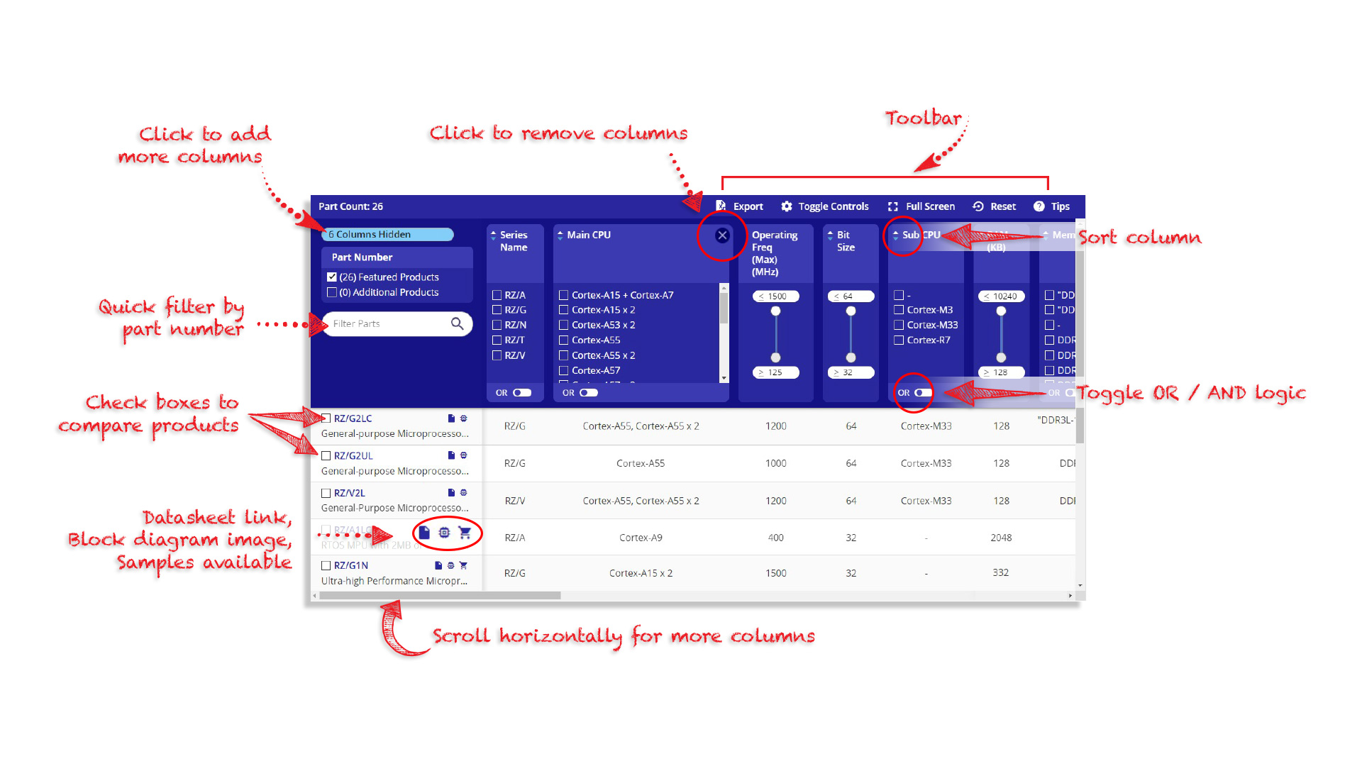
Tips for Using This Parametric Table:
- Hide Filters button in header: Collapse or expands filters
- Column sort buttons in header: Sort Column alphabetically / numerically descending or ascending
- Reset button in header: Reset all filters to the page default
- Full Screen button in header: Expand the table to full screen view (user must close out of full screen before they can interact with rest of page)
- Export button in header: Export the filtered results of the table to an Excel document
- Filter parts search bar in header: Type to filter table results by part number
- Hide column button in column headers: Select to hide columns in table
- AND / OR toggle switches in header: Toggles the logic of this particular filter to be “AND” or “OR” logic for filtering results
- Multiselect checkboxes at beginning of each row in table: Select these checkboxes to compare products against each other
- Document icon next to product name in row: View the featured document for this product
- Chip icon next to the right of the document icon in row: View the block diagram for this product
- Cart icon to the right of the chip icon: Indicates that samples are available for this product