概要
説明
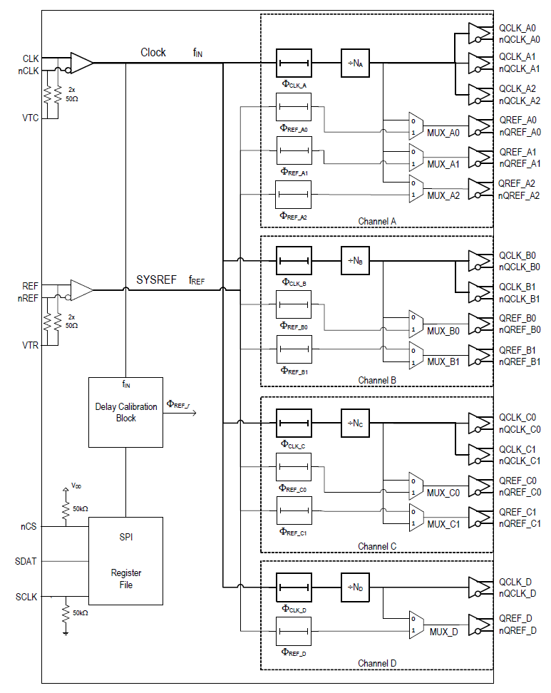
The 8V79S680 is a fully integrated, clock and SYSREF signal fanout buffer for JESD204B applications. It is designed as a high-performance clock and converter synchronization solution for wireless base station radio equipment boards with JESD204B subclass 0, 1 and 2 compliance. The main function of the device is the distribution and fanout of high-frequency clocks and low-frequency system reference signals generated by a JESB204B clock generator such as the 8V19N480, extending its fanout capabilities and providing additional phase-delay. The 8V79S680 is optimized to deliver very low phase noise clocks and precise, phase-adjustable SYSREF synchronization signals as required in GSM, WCDMA, LTE, LTE-A radio board implementations. Low-skew outputs, low device-to-device skew characteristics and fast output rise/fall times help the system design to achieve deterministic clock and SYSREF phase relationship across devices.
The device distributes the input clock and JESD204B SYSREF signals to four fanout channels. In each channel, both input clock and SYSREF signals are fanned-out to multiple clock (QCLK) and SYSREF (QREF) outputs. Clock signals can be frequency-divided in each channel. Configurable phase-delay circuits are available for both clock and SYSREF signals. The propagation delays in all signal paths are fully deterministic to support fixed phase relationships between clock and SYSREF signals within one device. Clock divider can be bypassed for low-latency clock paths. The device facilitates synchronization between frequency dividers within the device and across multiple devices, removing phase ambiguity introduced in dividers between power and configuration cycles.
Each channel supports clock frequencies up to 3GHz. In an alternative configuration, for instance JESD204B subclass 0 and 2, the SYSREF (QREF) outputs can be configured as regular clock outputs adding additional clock fanout to the device.
All outputs are very flexible in amplitude configuration, output signal termination and allow both DC and AC coupling. Outputs can be disabled and powered-down when not used. The SYSREF output pre-bias feature supports prevention of power-on glitches and enables AC-coupling of the system synchronization signals.
The device is configured through a 3-wire SPI serial interface. The device is packaged in a lead-free (RoHS 6) 64-lead VFQFN package. The extended temperature range supports wireless infrastructure, telecommunication and networking end equipment requirements. The device is a member of the high-performance clock family from IDT.
特長
- Supports high-speed, low phase noise converter clocks
- Distribution, fanout, phase-delay of clock and SYSREF signals
- Very low output noise floor: -158.8dBc/Hz noise floor (245.76MHz)
- Supports clock frequencies up to 3GHz, including clock output frequencies of 983.04MHz, 491.52MHz, 245.76MHz and 122.88MHz
- 4 output channels with a total of 16 differential outputs, organized in:
— 8 dedicated clock outputs
— 8 outputs configurable as SYSREF outputs with individual phase delay stages, or configurable as additional clock outputs - Each channel contains:
— frequency dividers: ÷1, ÷2, ÷4, ÷6, ÷8, ÷12, ÷16
— clock phase delay circuits - Clock phase delay circuits
— Clock: delay unit is the clock period; 256 steps
— SYSREF: Configurable precision phase delay circuits: 8 steps of 131ps, 262ps, 393ps or 524ps - Flexible differential outputs:
— LVDS/LVPECL configurable
— Amplitude configurable
— Power-down modes for unused outputs
— Supports DC and AC coupling
— QREF (SYSREF) output pre-bias feature to prevent glitches when turning output on or off - Supply voltage:
— 3.3V core and signal I/O
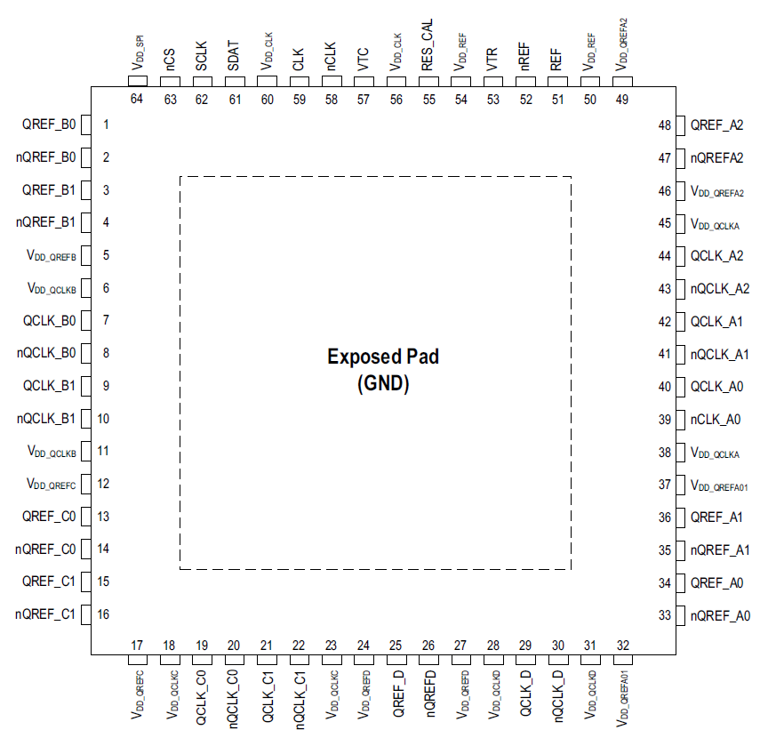
— 1.8V Digital control SPI I/O (3.3V-tolerant inputs) - 64 VFQFN-P package (9mm x 9mm x 0.85mm)
- Ambient temperature range: -40°C to +85°C
製品比較
アプリケーション
ドキュメント
= ピックアップ
ログイン後、ご登録が可能となります。
|
|
|
|
|---|---|---|
| 分類 | タイトル | 日時 |
| データシート | PDF 940 KB | |
| 製品変更通知 | PDF 1.26 MB | |
| 概要 | PDF 331 KB | |
| アプリケーションノート | PDF 601 KB | |
| アプリケーションノート | PDF 586 KB | |
| 製品変更通知 | PDF 983 KB | |
6 items
|
||
設計・開発
モデル
ECADモデル
[製品選択]テーブル内の製品名をクリックするとSamacSysが提供する回路図シンボル、PCBフットプリント、3D CADモデルがご確認いただけます。 お探しのシンボルやモデルが見つからない場合、Webサイトから直接リクエストできます。

Processing table
| VFQFPN | 64 | I | Yes | Tray | 3 | サンプルを入手, | ||
| VFQFPN | 64 | I | Yes | Reel | 3 |

Tips for Using This Parametric Table:
- Hide Filters button in header: Collapse or expands filters
- Column sort buttons in header: Sort Column alphabetically / numerically descending or ascending
- Reset button in header: Reset all filters to the page default
- Full Screen button in header: Expand the table to full screen view (user must close out of full screen before they can interact with rest of page)
- Export button in header: Export the filtered results of the table to an Excel document
- Filter parts search bar in header: Type to filter table results by part number
- Hide column button in column headers: Select to hide columns in table
- AND / OR toggle switches in header: Toggles the logic of this particular filter to be “AND” or “OR” logic for filtering results
- Multiselect checkboxes at beginning of each row in table: Select these checkboxes to compare products against each other
- Document icon next to product name in row: View the featured document for this product
- Chip icon next to the right of the document icon in row: View the block diagram for this product
- Cart icon to the right of the chip icon: Indicates that samples are available for this product
ビデオ&トレーニング
ニュース&ブログ
| ニュース | 2021年11月10日 |