图像


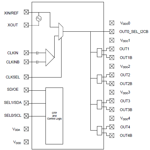
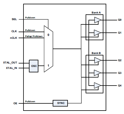
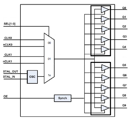
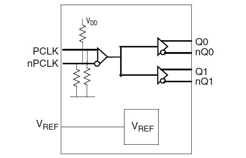
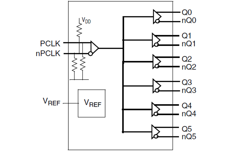
瑞萨电子时钟分配产品用于在使用或不使用锁相环路 (PLL) 的情况下,在系统中调节、操纵并分配时钟信号。 这些器件非常适合于大多数输入信号质量良好的应用,其目标是缓冲、扇出、分配或多路复用输入信号。 单输出时钟缓冲器还用于将时钟从一个信号标准转化成另一个标准(例如,将 LVCMOS 输入转化成 LVPECL 输出)。
作为计时解决方案的行业领导者,瑞萨提供丰富的时钟缓冲器、时钟分配和多路复用器解决方案组合,可满足几乎任何应用的需求。 瑞萨拥有最广泛的时钟分配器件产品组合,可支持差分信号。 这些器件支持的最常见的 I/O 级信号包括 LVDS、LVPECL、HCSL、LVCMOS、CML、HSTL、SSTL 等。
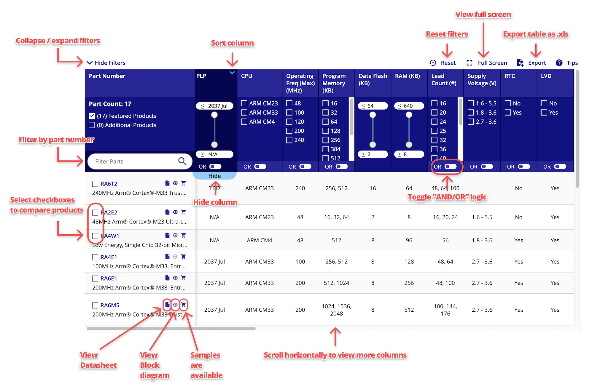
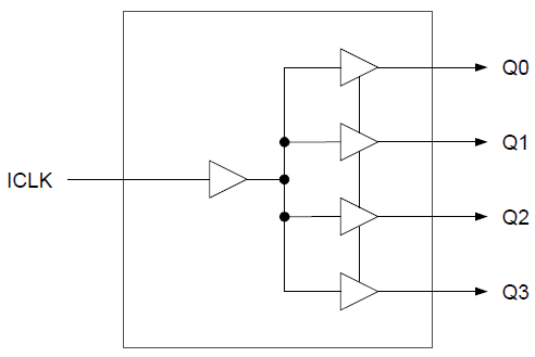
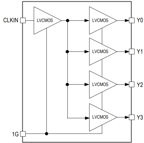
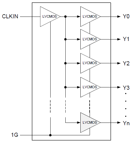
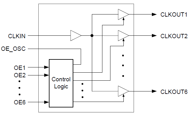
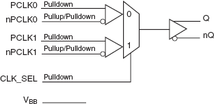
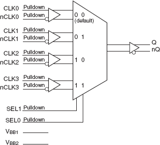
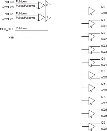
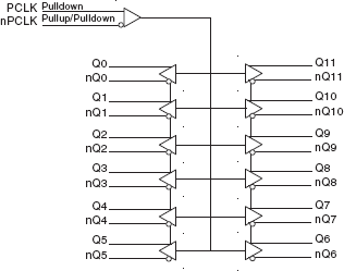
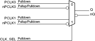
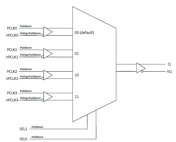
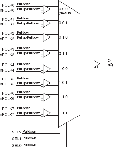
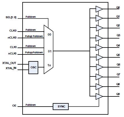
时钟分配器件可采用多种方法分类。 在某些情况下,设计人员可能希望获得输入时钟,然后将其分配给多个目标,而无需修改时钟频率。 在其它情况下,设计人员可能需使用其它时钟对其进行分频或复用。
另外,在一些时钟分配应用中可能需要零延迟缓冲器。 零延迟缓冲器是基于 PLL 的器件,可重新生成带有扇出的输入时钟信号以驱动多个负载。 大多数器件的延迟可通过外部反馈路径进行调节。
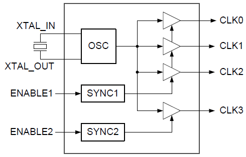
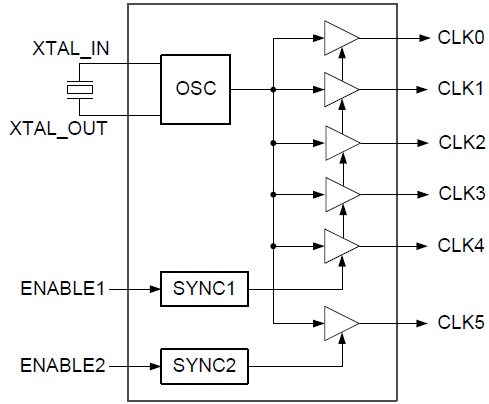
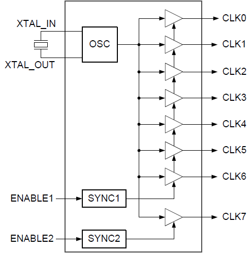
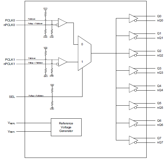
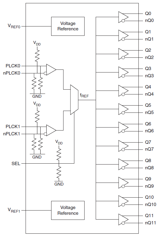
关于时钟分配网络
时钟分配网络(通常称为时钟树)可将来自一个共同来源的时钟信号分配至需要信号的所有电气元件。 此功能对于同步系统的操作非常重要,为了实现时钟信号及其分配中使用的电气网络的特征,必须对该功能给予足够的重视。 对时钟分配网络进行适当设计可以确保关键计时要求得到满足,从而实现可靠操作和最佳性能。
Subcategory |
Temp. Range |
Pkg. Type |
Lead Count (#) |
Pkg. Dimensions (mm) |
|
|---|---|---|---|---|---|
| 器件号 | |||||
| Low Skew 1 to 4 Clock Buffer | Clock Buffers & Drivers | -40 to 85°C | COL, SOIC | 8 | 2.0 x 2.0 x 0.5, 4.9 x 3.9 x 1.5 |
| Low Skew 1 to 4 Clock Buffer | Clock Buffers & Drivers | -40 to 85°C | COL, SOIC | 8 | 2.0 x 2.0 x 0.5, 4.9 x 3.9 x 1.5 |
| Programmable Fanout Buffer | Clock Buffers & Drivers | -40 to 85°C | VFQFPN | 24 | 4.0 x 4.0 x 0.9 |
| Programmable Fanout Buffer | Clock Buffers & Drivers | -40 to 85°C | VFQFPN | 24 | 4.0 x 4.0 x 0.9 |
| 1.8 V to 3.3 V 1:4 Crystal Input to LVCMOS Output High-Performance Clock Fanout Buffer with OE | Clock Buffers & Drivers | -40 to 105°C | COL, TSSOP | 16 | 2.5 x 2.5 x 0.5, 5.0 x 4.4 x 1.0 |
| 1.8 V to 3.3 V 1:6 Crystal Input to LVCMOS Output High-Performance Clock Fanout Buffer with OE | Clock Buffers & Drivers | -40 to 105°C | COL, TSSOP | 16 | 2.5 x 2.5 x 0.5, 5.0 x 4.4 x 1.0 |
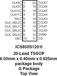
| 1.8 V to 3.3 V 1:8 Crystal Input to LVCMOS Output High-Performance Clock Fanout Buffer with OE | Clock Buffers & Drivers | -40 to 105°C | TSSOP, VFQFPN | 20 | 3.0 x 3.0 x 1.0, 6.5 x 4.4 x 1.0 |
| 1.8V to 3.3V 1:2 LVCMOS High Performance Clock Buffer | Clock Buffers & Drivers | -40 to 85°C, -40 to 105°C | COL, TSSOP | 8 | 2.0 x 2.0 x 0.5, 3.1 x 4.4 x 1.0 |
| 1.8 V to 3.3 V 1:4 LVCMOS High Performance Clock Buffer | Clock Buffers & Drivers | -40 to 85°C, -40 to 105°C, -40 to 125°C | COL, TSSOP | 8 | 2.0 x 2.0 x 0.5, 2.0 x 2.0 x 0.75, 3.1 x 4.4 x 1.0 |
| 1.8 V to 3.3 V 1:6 LVCMOS High Performance Clock Buffer | Clock Buffers & Drivers | -40 to 85°C, -40 to 105°C | COL, TSSOP | 14, 16 | 2.5 x 2.5 x 0.5, 5.0 x 4.4 x 1.0 |
| 1.8 V to 3.3 V 1:8 LVCMOS High Performance Clock Buffer | Clock Buffers & Drivers | -40 to 85°C, -40 to 105°C | COL, TSSOP | 16 | 2.5 x 2.5 x 0.5, 5.0 x 4.4 x 1.0 |
| 1.8 V to 3.3 V 1:10 LVCMOS High Performance Clock Buffer | Clock Buffers & Drivers | -40 to 85°C, -40 to 105°C | TSSOP, VFQFPN | 20 | 3.0 x 3.0 x 1.0, 6.5 x 4.4 x 1.0 |
| 1.8 V 1:3 TCXO / LVCMOS High-Performance Clock Buffer | Clock Buffers & Drivers | -40 to 105°C | DFN | 10 | 2.0 x 2.0 x 0.75 |
| 1.8 V 1:4 TCXO / LVCMOS High-Performance Clock Buffer | Clock Buffers & Drivers | -40 to 105°C | COL | 16 | 2.5 x 2.5 x 0.5 |
| 1.8 V 1:6 TCXO / LVCMOS High-Performance Clock Buffer | Clock Buffers & Drivers | -40 to 105°C | VFQFPN | 20 | 3.0 x 3.0 x 1.0 |
| 2.5 V to 3.3 V 1:3 TCXO / LVCMOS High-Performance Clock Buffer | Clock Buffers & Drivers | -40 to 105°C | DFN | 10 | 2.0 x 2.0 x 0.75 |
| 2.5 V to 3.3 V 1:4 TCXO / LVCMOS High-Performance Clock Buffer | Clock Buffers & Drivers | -40 to 105°C | COL | 16 | 2.5 x 2.5 x 0.5 |
| 2.5 V to 3.3 V 1:6 TCXO / LVCMOS High-Performance Clock Buffer | Clock Buffers & Drivers | -40 to 105°C | VFQFPN | 20 | 3.0 x 3.0 x 1.0 |
| 12:1 Single-Ended Multiplexer | Clock Multiplexers (MUX) | -40 to 85°C | TSSOP | 20 | 6.5 x 4.4 x 1.0 |
| Low Skew,1-to-6,Differential-to-2.5V,3.3V LVPECL/ECL Fanout Buffer | Clock Buffers & Drivers | -40 to 85°C | TSSOP | 20 | 6.5 x 4.4 x 1.0 |
| Low Skew,1-to-2,Differential-to-2.5V,3.3V LVPECL/ECL Fanout Buffer | Clock Buffers & Drivers | -40 to 85°C | SOIC, TSSOP | 8 | 3.0 x 3.0 x 0.97, 4.9 x 3.9 x 1.5 |
| 12:1 Differential-to-3.3V,2.5V LVPECL Clock/Data Multiplexer | Clock Multiplexers (MUX) | -40 to 85°C | VFQFPN | 32 | 5.0 x 5.0 x 0.9 |
| Low Skew,1-to-5 Differential-to-2.5V,3.3V LVPECL/ECL Fanout Buffer | Clock Buffers & Drivers | -40 to 85°C | TSSOP | 20 | 6.5 x 4.4 x 1.0 |
| 2:1 Differential-to-LVPECL Multiplexer | Clock Multiplexers (MUX) | -40 to 85°C | TSSOP, VFQFPN | 16 | 3.0 x 3.0 x 1.0, 5.0 x 4.4 x 1.0 |
| 4:1 Differential-to-3.3V, 2.5V LVPECL / ECL Clock Multiplexer | Clock Multiplexers (MUX) | -40 to 85°C | TSSOP | 20 | 6.5 x 4.4 x 1.0 |
| Low Skew, 1-to-10 Differential-to-2.5V, 3.3V LVPECL / ECL Fanout Buffer | Clock Buffers & Drivers | -40 to 85°C | VFQFPN | 32 | 5.0 x 5.0 x 0.9 |
| Low Skew,1-to-12,Differential-to-3.3V,2.5V LVPECL Fanout Buffer | Clock Buffers & Drivers | -40 to 85°C | VFQFPN | 32 | 5.0 x 5.0 x 0.9 |
| 2:1 Differential-to-LVDS Multiplexer | Clock Multiplexers (MUX) | -40 to 85°C | VFQFPN | 16 | 3.0 x 3.0 x 1.0 |
| 4:1 Differential-to-LVDS Clock Multiplexer | Clock Multiplexers (MUX) | -40 to 85°C | TSSOP | 16 | 5.0 x 4.4 x 1.0 |
| 8:1 Differential-to-LVDS Clock Multiplexer | Clock Multiplexers (MUX) | -40 to 85°C | TSSOP | 24 | 7.8 x 4.4 x 1.0 |
| Crystal or Differential to LVCMOS/ LVTTL Clock Buffer | Clock Buffers & Drivers | -40 to 85°C | VFQFPN | 32 | 5.0 x 5.0 x 0.9 |
| Crystal or Differential to LVCMOS/ LVTTL Clock Buffer | Clock Buffers & Drivers | -40 to 85°C | VFQFPN | 24 | 4.0 x 4.0 x 0.9 |
| Crystal or Differential to LVCMOS/ LVTTL Clock Buffer | Clock Buffers & Drivers | -40 to 85°C | VFQFPN | 32 | 5.0 x 5.0 x 0.9 |
| 1:2 LVDS 1.8V / 2.5V Fanout Buffer for 1PPS and High-Speed Clocks | RF Buffers | -40 to 85°C | VFQFPN | 16 | 3.0 x 3.0 x 1.0 |
| 1:6 LVDS Output 1.8V Fanout Buffer | RF Buffers | -40 to 85°C | VFQFPN | 20 | 4.0 x 4.0 x 1.0 |
| 2:4 LVDS 1.8V / 2.5V Fanout Buffer for 1PPS and High-Speed Clocks | RF Buffers | -40 to 85°C | VFQFPN | 16 | 3.0 x 3.0 x 1.0 |
| 2:8 LVDS 1.8V / 2.5V Fanout Buffer for 1PPS and High-Speed Clocks | RF Buffers | -40 to 85°C | VFQFPN | 28 | 5.0 x 5.0 x 0.8 |
| 2:12 LVDS 1.8V / 2.5V Fanout Buffer for 1PPS and High-Speed Clocks | RF Buffers | -40 to 85°C | VFQFPN | 40 | 6.0 x 6.0 x 0.9 |
| Dual 1:2 LVDS 1.8V / 2.5V Fanout Buffer for 1PPS and High-Speed Clocks | RF Buffers | -40 to 85°C (Tc ≤ 105°C) | VFQFPN | 16 | 3.0 x 3.0 x 1.0 |
| Dual 1:4 LVDS 1.8V / 2.5V Fanout Buffer for 1PPS and High-Speed Clocks | RF Buffers | -40 to 85°C (Tc ≤ 105°C) | VFQFPN | 28 | 5.0 x 5.0 x 0.8 |
| Dual 1:6 LVDS Output 1.8V / 2.5V Fanout Buffer | RF Buffers | -40 to 85°C (Tc ≤ 105°C) | WLCSP | 48 | 3.59 x 3.04 x 0.6 |
| Dual 1:6 LVDS Output 1.8V / 2.5V Fanout Buffer | RF Buffers | -40 to 85°C | VFQFPN | 40 | 6.0 x 6.0 x 0.9 |
| Dual 1:8 LVDS 1.8V / 2.5V Fanout Buffer for 1PPS and High-Speed Clocks | RF Buffers | -40 to 85°C (Tc ≤ 105°C) | VFQFPN | 48 | 7.0 x 7.0 x 0.9 |
| Low Additive Jitter 2:8 Buffer with Universal Differential Outputs | Clock Buffers & Drivers | -40 to 85°C | VFQFPN | 32 | 5.0 x 5.0 x 0.9 |
| Low Additive Jitter 2:8 Buffer with CMOS / Differential Outputs | Clock Buffers & Drivers | -40 to 85°C | VFQFPN | 32 | 5.0 x 5.0 x 0.9 |
| Programmable Low Additive Jitter 2:8 Buffer with Dividers and Universal Outputs | Clock Buffers & Drivers | -40 to 85°C | VFQFPN | 32 | 5.0 x 5.0 x 0.9 |
| 2:4, LVDS Output Fanout Buffer, 2.5V | RF Buffers | -40 to 85°C | VFQFPN | 16 | 3.0 x 3.0 x 1.0 |
| 2:4, LVDS Output Fanout Buffer, 3.3 V | RF Buffers | -40 to 85°C | VFQFPN | 16 | 3.0 x 3.0 x 1.0 |
| 1:8, LVDS Output Fanout Buffer | RF Buffers | -40 to 85°C | VFQFPN | 28 | 5.0 x 5.0 x 0.8 |
| 1:12, LVDS Output Fanout Buffer | RF Buffers | -40 to 85°C | VFQFPN | 40 | 6.0 x 6.0 x 0.9 |
| 新闻 | 2022年4月14日 |
