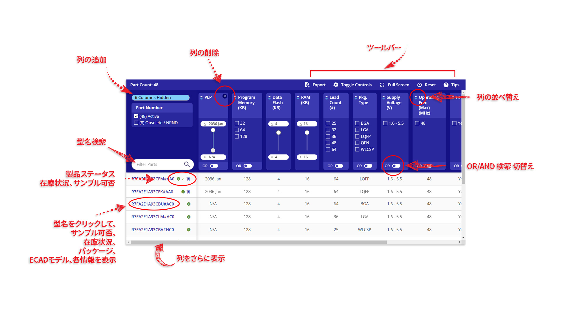
画像


窒化ガリウム電界効果トランジスタ(GaN FET)のようなワイドバンドギャップ半導体技術は、航空宇宙アプリケーションにおけるパワーマネジメントや電力変換に役立つものとして関心を集めています。 これらのデバイスは絶縁破壊電圧、低いRDS(ON)、極めて低いゲート電荷を特長としており、高効率化や省スペースソリューションフットプリントを実現しながら高いスイッチング周波数で操作できるパワーマネジメントシステムを可能にします。 GaNデバイスには、航空宇宙市場にとって魅力的なもう1つの利点があります。 これらのデバイスは本来、イオン化線量合計に対して免疫があります。
ルネサスの 耐放射線強化ポートフォリオには、人工衛星やその他の過酷環境アプリケーション向けのGaN FETが含まれます。 GaN FETは、より優れた導電性とスイッチング特性を有するため、システムのサイズ、重量、電力損失の削減など、システムの利便性を高めます。
| 40V, 65A Enhancement Mode GaN Power Transistor | 40 | 65 | 2.5 | 6 | 3.5 | 19 | 3.1 | 100 | 75 | 86 | 4 | CLCC, PFL | -55 to 125°C | Modified Class V, PROTO | SPICE |
| 100V, 60A Enhancement Mode GaN Power Transistor | 100 | 60 | 2.5 | 6 | 5 | 2.5 | 3.1 | 100 | 75 | 86 | 4 | CLCC | -55 to +125°C, -55 to 125°C | Modified Class V, PROTO | SPICE |
| 200V, 7.5A Enhancement Mode GaN Power Transistor | 200 | 7.5 | 2.5 | 6 | 45 | 14 | 18.7 | 100 | 75 | 86 | 4 | CLCC, PFL | -55 to +125°C, -55 to 125°C | Modified Class V, PROTO | SPICE |
| 40V, 65A Enhancement Mode GaN Power Transistor | 40 | 65 | 2.5 | 6 | 3.5 | 19 | 3.1 | 75 | 86 | 4 | CLCC, PFL | -55 to 125°C | Modified Class V, PROTO | ||
| 100V, 60A Enhancement Mode GaN Power Transistor | 100 | 60 | 2.5 | 6 | 5 | 2.5 | 3.1 | 100 | 75 | 86 | 4 | CLCC, PFL | -55 to +125°C, -55 to 125°C | Modified Class V, PROTO | SPICE |
| 200V, 7.5A Enhancement Mode GaN Power Transistors | 200 | 7.5 | 2.5 | 6 | 45 | 14 | 18.7 | 75 | 86 | 4 | CLCC, PFL | -55 to +125°C, -55 to 125°C | Modified Class V, PROTO | SPICE |
|
|
|
|
|---|---|---|
| 分類 | タイトル | 日時 |
| カタログ | PDF 467 KB | |
| カタログ | PDF 4.85 MB | |
| 技術概要 | PDF 332 KB | |
| アプリケーションノート | PDF 221 KB | |
| ホワイトペーパー | PDF 1.49 MB 英語 | |
| ホワイトペーパー | PDF 548 KB | |
| アプリケーションノート | PDF 338 KB | |
7 items
|
||
Renesas, a leading solution provider in the satellite and high reliability industry, discusses a technology leap into Gallium Nitride with its family of Intersil GaN products. The ISL70024SEH is designed from the ground up with space applications in mind to provide steady and reliable performance when exposed to total ionizing dose (TID) or heavy ions. The Intersil GaN driver and FET together allow more efficient switching, higher frequency operation, reduced gate drive voltage and a smaller solution size compared to their traditional silicon counterparts.
Renesas is a leading solution provider in the satellite and high reliability industry, and is now introducing a technology leap into Gallium Nitride with its new family of GaN products.
GaN is a wideband gap material and compared to silicon, the drain to source distance can be a factor of ten smaller which translates to a much smaller RDS(on). While silicon FETs are very close to their theoretical limit of channel length, GaN has much more room for improvement. GaN's advantages to the power supply designers include size, weight and efficiency.
The size and weight reduction of using GaN over silicon comes from two factors. The first is that heat-sinking requirements are not as much due to GaN's reduced parasitics. And the second, is the use of smaller output filters due to being able to switch at higher frequencies. This allows GaN to achieve excellent efficiencies at a compact solution size.
Another plus point, when it comes to ionizing radiation in contrast to silicon FETs, GaN FETS do not have a gate oxide layer. That means radiation cannot form traps in the gate oxide that would otherwise shift the gate to source threshold voltage.
As you can see in the graph, the current technology of GaN is already orders of magnitude better and figure of merit, and this will only get better with time. To be able to take full advantage of GaN FETs, you'll need a good gate driver to go with it. So Renesas is now introducing the industry's first radiation hardened low-side GaN FET driver.
A GaN FET gate driver needs to provide a well-regulated gate voltage that never exceeds 6V under all conditions. The ISL70040SEH regulates a 4.5V gate driver in order to meet the voltage margins of the space and high reliability industry.
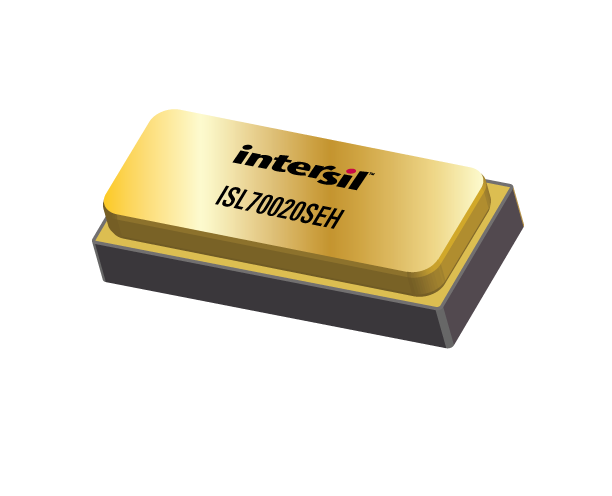
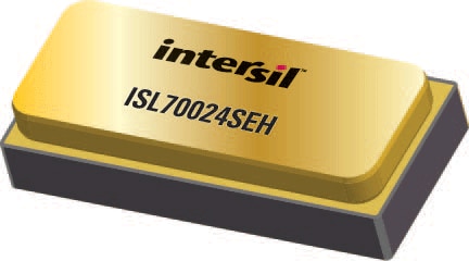
Here we have the ISL70040SEH low-side driver and the ISL70024SEH, the 200V GaN FET, in action. The VDD is set to 5V and the inputs are driven with a function generator set to a frequency of 500kHz. As you can see, it has fast transition times with minimal overshoot on the rising and falling edges with a well-regulated 4.5V gate drive voltage.
It is designed from the ground up with space applications in mind to provide steady and reliable performance when exposed to total ionizing dose (TID) or heavy ions. This first graph shows minimal shift in V drive, the gate drive voltage across TID for both high dose rate and low dose rate. The next graph shows how steady the operating supply current is across TID. For both gate drive voltage and supply current, we are well within the spec limits. From a single event transient perspective, at an LET limit of 86MeV, the ISL70040SEH had a very small cross section of ≤1.7 x 10⁻⁶cm2 for dynamic switching, and had no SETs for static input, high or low.
GaN FETS are a very good fit for satellite applications but require a good gate driver to realize their full potential. Together they allow more efficient switching, higher frequency operation, reduced gate drive voltage and a smaller solution size compared to their traditional silicon counterparts.
For more information, datasheets, TID/SEE test reports, or to order parts or evaluation boards, please visit our Rad Hard GaN FET product page.