

Does it seem to you that every design has a common issue? There always seems to be a timing reference that is missing and designers are left wondering ‘why didn’t they include one more output on their clock generator, or two, or 10!?’ How am I going to route all these timing signals across my board!? And each generation of their boards has more of them.
Yes, it’s apparent that clock buffers will have a long and successful future. But they follow Darwin’s theory. Only the buffers that adapt may survive the system engineering litmus test. Are they useful and do they simplify the timing chain design? Do they work seamlessly with the rest of the timing chain and standout due to their capabilities and differentiation in the signal chain (size, power, low jitter, and cost of ownership)?
This is one aspect of their design that customers have long relied on Renesas for – to provide the largest variety of buffers with quality, excellent performance, highest versatility or to meet very specific system requirements. In other words, the buffer seems to have been made just for them.
Renesas has the broadest portfolio of high-performance buffers in the industry, and in this blog, I will provide a review of a very useful family of simple but powerful buffers. These are well-suited for many different applications, particularly in the wireline communications space.
1PPS or higher with barely any jitter impact, high flexibility, in a tiny footprint
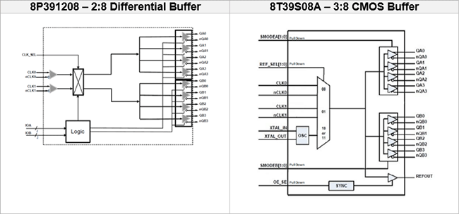
Let’s start with the 8P39xx (differential) and the 8P79xx (differential plus CMOS) devices. Both of these families have been tailored to wireline applications and designed to also support 1PPS signals for applications supporting synchronization and distribution of those signals. By avoiding internal AC coupling, the VOH and VOL do not drift when operating at a low enough frequency such as 1PPS. They also cover most or all frequencies used in wireline applications. These buffers also have a very advantageous low power-to-high fanout ratio to ease system thermal constraints. Each bank can operate at different VDDOs, so the user can tailor each output bank to a specific usage. Glitchless output Disable functions are provided to avoid runt pulse generation when enabling or disabling an output.
Flexibility is provided with pin strapping, so no serial programming is required. Differential input pairs can accept input levels such as LVPECL, LVDS, HCSL, HSTL and single-ended, and the format for each bank of outputs can be selectable as LVPECL, LVDS, CML or HCSL. Renesas offers all this flexibility, excellent 50 fs max additive jitter and low noise floor in a very small footprint, too.
Do you use a crystal input? No problem. The 8T39Sxx family will add an integrated crystal oscillator in addition to offering a typical additive jitter performance of 35 fs RMS (12 kHz to 20 MHz integration range), and 80ps maximum output to output skew.
8P391208 and 8T39S08A – two examples of high-performance 8-output buffers
Benefits:
- Designed for high-performance wireline applications
- Designed to support 1 PPS for synchronization applications
- Lowest power with high fanout
- Very low additive jitter for best SNR, data rate optimization and low BER
- No programming needed – power up ready (3-state pin)
- Flexibility for lower cost of ownership (format, 1 or 2 integrated buffers)
Just need a very simple but high-performance CMOS buffer?
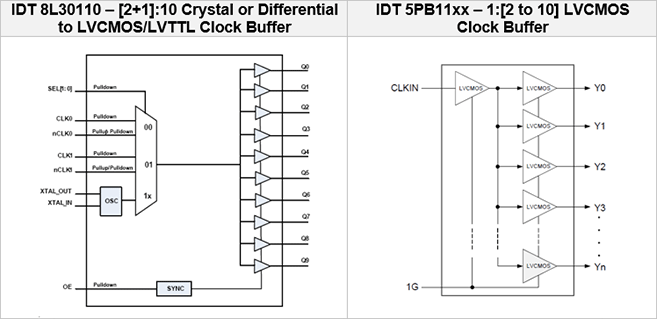
Renesas offers the 8L301xx family of CMOS buffers. For example, the 8L30110 offers up to 10 outputs in a 5x5 package, with all the essential functionality, but no more. Typical additive jitter of 24 fs barely impacts the total jitter budget for the application. Glitchless OE and XTAL oscillators are also provided. These buffers also offer an input multiplexer so the user can select between two different inputs or an XTAL input.
Renesas also offers another family of even simpler CMOS buffers, the 5PB11xx family consisting of five clock fanout buffer members where the two last digits represent the number of outputs. These buffers are very high performance, low jitter, low skew and propagation delay, very low power straight CMOS fanout buffers.
High-performance low power CMOS Clock Fanout buffers – Examples of 8L30110 and 5PB11xx family
Benefits:
- Designed for high-performance wireline applications
- Very low power allows distribution with little concerns for thermals and power/heat dissipation
- Very low additive jitter with almost no impact on total jitter budget
- No programming needed – power up ready
- 8L30xx family offers possibility of XTAL input and an input multiplexer
- 5PB11xx supports 1PPS distribution
- 5PB11xx family has fully characterized propagation delay
- TSSOP and DFN/QFN packages, as small as 2 × 2 mm
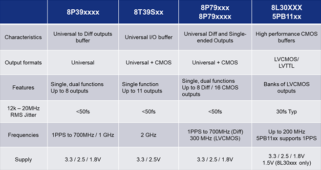
Clock Buffer Family Overview
Engineers have found these buffers very practical and helpful in a series of applications including:
- GPON OLT and DSL DSLAM for the low power, voltage and format flexibility and jitter performance
- PTN/OTN and Core Networks for performance and flexibility
- Enterprise switches with easy clock distribution to FPGAs and Ethernet PHYs
- Datacenters for performance, power and simplicity
- PON ONT or DSL CPE for cost effectiveness, low power, and small form factors of the CMOS buffer families, and internal crystal oscillator
Visit renesas.com/buffers to see the complete portfolio of high-performance buffers from Renesas.