
概要
説明
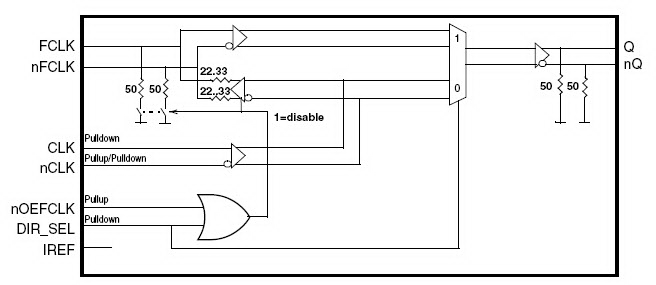
The 831752I is a high-performance, differential HCSL clock switch. The device is designed for the routing of PCIe clock signals in ATCA/AMC system and is optimized for PCIe Gen 1, Gen 2 and Gen 3. The device has one differential, bi-directional I/O (FCLK) for connection to ATCA clock sources and to clock receivers through a connector. The differential clock input CLK is the local clock input and the HCSL output Q is the local clock output. In the common clock mode, FCLK serves as an input and is routed to the differential HCSL output Q. There are two local clock modes. In the local clock mode 0, CLK is the input, Q is the clock output and FCLK is in high-impedance state. In the local clock mode 1, CLK is the input and both Q and FCLK are the outputs of the locally generated PCIe clock signal. The 831752I is characterized to operate from a 3.3V power or 2.5V power supply. The 831752I supports the switching of PCI Express (2.5 Gb/s), Gen 2 (5 Gb/s) and Gen 3 (8 Gb/s) clock signals.
特長
- Clock switch for PCIe and ATCA/AMC applications
- Supports local and common ATCA/AMC clock modes
- Bi-directional clock I/O FCLK: -When operating as an output, FCLK is a source-terminated HCSL signal. - When operating as an input, FCLK accepts HCSL, LVDS and LVPECL levels.
- Local clock input (CLK) accepts HCSL, LVDS and LVPECL differential signals
- Local HCSL clock output (Q)
- Maximum input/output clock frequency: 500MHz
- Maximum input/output data rate: 1000Mb/s (NRZ)
- LVCMOS interface levels for the control inputs
- PCI Express (2.5 Gb/S), Gen 2 (5 Gb/s) and Gen 3 (8 Gb/s) jitter compliant
- Full 3.3V or 2.5V supply voltage
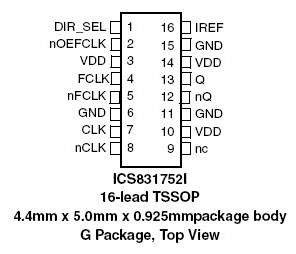
- Lead-free (RoHS 6) 16-lead TSSOP package
- -40°C to 85°C ambient operating temperature
製品比較
アプリケーション
設計・開発
モデル
ECADモデル
[製品選択]テーブル内の製品名をクリックするとSamacSysが提供する回路図シンボル、PCBフットプリント、3D CADモデルがご確認いただけます。 お探しのシンボルやモデルが見つからない場合、Webサイトから直接リクエストできます。

Processing table
| TSSOP | 16 | I | Yes | Tube | ||
| TSSOP | 16 | I | Yes | Reel |

Tips for Using This Parametric Table:
- Hide Filters button in header: Collapse or expands filters
- Column sort buttons in header: Sort Column alphabetically / numerically descending or ascending
- Reset button in header: Reset all filters to the page default
- Full Screen button in header: Expand the table to full screen view (user must close out of full screen before they can interact with rest of page)
- Export button in header: Export the filtered results of the table to an Excel document
- Filter parts search bar in header: Type to filter table results by part number
- Hide column button in column headers: Select to hide columns in table
- AND / OR toggle switches in header: Toggles the logic of this particular filter to be “AND” or “OR” logic for filtering results
- Multiselect checkboxes at beginning of each row in table: Select these checkboxes to compare products against each other
- Document icon next to product name in row: View the featured document for this product
- Chip icon next to the right of the document icon in row: View the block diagram for this product
- Cart icon to the right of the chip icon: Indicates that samples are available for this product