
1.8 V 1:3 TCXO / LVCMOS High-Performance Clock Buffer
ページセクションへ移動:
概要
説明
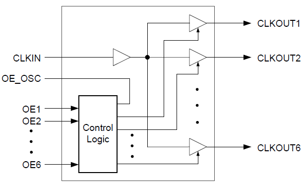
The 5PB1203 is a high-performance TCXO / LVCMOS clock fanout buffer with individual OE pin for each output. The CLKIN pin can accept either a square wave (LVCMOS) or clipped sine wave (such as TCXO clipped sine wave output) as input.
The 5PB1203 has industry-leading low jitter and extremely low current consumption, making it ideal for smart mobile devices.
The 5PB1203 has industry-leading low jitter and extremely low current consumption, making it ideal for smart mobile devices.
特長
- Extremely low operating and standby current consumption
- Low RMS Additive Phase jitter
- 1.8 V power supply voltage
- Three outputs with individual Output Enable pin
- One input
- OE_OSC control pin to enable/disable reference TCXO / XO
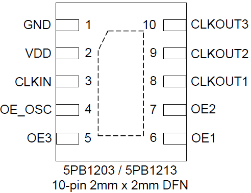
- Small 10-pin DFN package
- Extended temperature range (-40°C to +105°C)
製品比較
アプリケーション
ドキュメント
= ピックアップ
ログイン後、ご登録が可能となります。
|
|
|
|
|---|---|---|
| 分類 | タイトル | 日時 |
| データシート | PDF 292 KB | |
| アプリケーションノート | PDF 187 KB | |
| 概要 | PDF 217 KB | |
| 製品変更通知 | PDF 129 KB | |
| 概要 | PDF 252 KB | |
| アプリケーションノート | PDF 495 KB | |
| アプリケーションノート | PDF 442 KB | |
| アプリケーションノート | PDF 565 KB | |
8 items
|
||
設計・開発
モデル
ECADモデル
[製品選択]テーブル内の製品名をクリックするとSamacSysが提供する回路図シンボル、PCBフットプリント、3D CADモデルがご確認いただけます。 お探しのシンボルやモデルが見つからない場合、Webサイトから直接リクエストできます。

Processing table
| DFN | 10 | K | Yes | Cut Tape | 1 | 0.9666 | サンプルを入手, | |
| DFN | 10 | K | Yes | Reel | 1 |

Tips for Using This Parametric Table:
- Hide Filters button in header: Collapse or expands filters
- Column sort buttons in header: Sort Column alphabetically / numerically descending or ascending
- Reset button in header: Reset all filters to the page default
- Full Screen button in header: Expand the table to full screen view (user must close out of full screen before they can interact with rest of page)
- Export button in header: Export the filtered results of the table to an Excel document
- Filter parts search bar in header: Type to filter table results by part number
- Hide column button in column headers: Select to hide columns in table
- AND / OR toggle switches in header: Toggles the logic of this particular filter to be “AND” or “OR” logic for filtering results
- Multiselect checkboxes at beginning of each row in table: Select these checkboxes to compare products against each other
- Document icon next to product name in row: View the featured document for this product
- Chip icon next to the right of the document icon in row: View the block diagram for this product
- Cart icon to the right of the chip icon: Indicates that samples are available for this product
ビデオ&トレーニング
5PB11xx Ultra Low Jitter LVCMOS Buffers
This video provides an overview of the LVCMOS High Performance Clock Buffer Family, highlighting their key features and capabilities.

Video List
ニュース&ブログ
| IDT社が超低ジッターのLVCMOSクロックバッファ製品ファミリーを開発 | ニュース | 2015年3月30日 |