
CMOS Dual 4-Stage Static Shift Register With Serial Input/Parallel Output
跳转至页面部分:
概览
简介
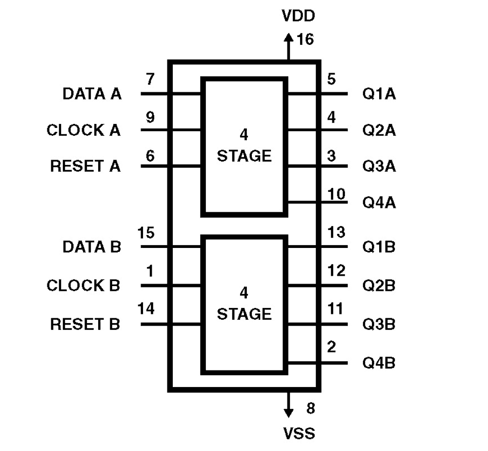
CD4015BMS consists of two identical, independent, 4-stage serial-input/parallel output registers. Each register has independent CLOCK and RESET inputs as well as a single serial DATA input. Q outputs are available from each of the four stages on both registers. All register stages are D type, master-slave flip-flops. The logic level present at the DATA input is transferred into the first register stage and shifted over one stage at each positive-going clock transition. Resetting of all stages is accomplished by a high level on the reset line. Register expansion to 8 stages using one CD4015BMS package, or to more than 8 stages using additional CD4015BMS's is possible. The CD4015BMS is supplied in these 16 lead outline packages: Braze Seal DIP H4X Frit Seal DIP H1F Ceramic Flatpack H6W
特性
- High voltage type (20V rating)
- Medium speed operation 12MHz (typ.) clock rate at VDD - VSS = 10V
- Fully static operation
- 8 master-slave flip-flops plus input and output buffering
- 100% tested for quiescent current at 20V
- 5V, 10V and 15V parametric ratings
- Standardized symmetrical output characteristics
- Maximum input current of 1µA at 18V over full package - temperature range; 100nA at 18V and 25 °C
- Noise margin (full package - temperature range) = 1V at VDD = 5V, 2V at VDD = 10V, 2.5V at VDD = 15V
- Meets all requirements of JEDEC tentative standard No. 13B, "Standard Specifications for Description of 'B' Series CMOS Devices"
产品对比
应用
应用
- Serial-input/parallel-output data queueing
- Serial to parallel data conversion
- General-purpose register
文档
= 相关文档
请登录后开启订阅
|
|
|
|
|---|---|---|
| 类型 | 文档标题 | 日期 |
| 数据手册 | PDF 415 KB | |
| 手册 | PDF 467 KB | |
| 手册 | PDF 4.85 MB | |
| Price Increase Notice | PDF 360 KB | |
| 其他 | ||
| 白皮书 | PDF 533 KB | |
| Product Advisory | PDF 499 KB | |
| 产品变更通告 | PDF 230 KB | |
| 应用文档 | PDF 338 KB | |
9 items
|
||
设计和开发
模型
ECAD 模块
Schematic symbols, PCB footprints, and 3D CAD models from SamacSys can be found by clicking on products in the Product Options table. If a symbol or model isn't available, it can be requested directly from the website.

Processing table

Tips for Using This Parametric Table:
- Hide Filters button in header: Collapse or expands filters
- Column sort buttons in header: Sort Column alphabetically / numerically descending or ascending
- Reset button in header: Reset all filters to the page default
- Full Screen button in header: Expand the table to full screen view (user must close out of full screen before they can interact with rest of page)
- Export button in header: Export the filtered results of the table to an Excel document
- Filter parts search bar in header: Type to filter table results by part number
- Hide column button in column headers: Select to hide columns in table
- AND / OR toggle switches in header: Toggles the logic of this particular filter to be “AND” or “OR” logic for filtering results
- Multiselect checkboxes at beginning of each row in table: Select these checkboxes to compare products against each other
- Document icon next to product name in row: View the featured document for this product
- Chip icon next to the right of the document icon in row: View the block diagram for this product
- Cart icon to the right of the chip icon: Indicates that samples are available for this product