-
-
设计资源
- 设计和开发
- 特色设计工具
- 合作伙伴
- 内容和培训
9170B-01
circle过时Clock Synchronizer and Multiplier
跳转至页面部分:
arrow_drop_down
概览
简介
The IDT9170B generates an output clock which is synchronized to a given continuous input clock with zero delay (±1ns at 5 V VDD). Using IDT's proprietary phase-locked loop (PLL) analog CMOS technology, the IDT9170B is useful for regenerating clocks in high speed systems where skew is a major concern. By the use of the two select pins, multiples or divisions of the input clock can be generated with zero delay (see Tables 2 and 3). The standard versions produce two outputs, where CLK2 is always a divide by two version of CLK1. The IDT9170B is also useful to recover poor duty cycle clocks. A 50 MHz signal with a 20/80% duty cycle, for example, can be regenerated to the 48/52% typical of the part. The IDT9170B allows the user to control the PLL feedback, making it possible, with an additional 74F240 octal buffer (or other such device that offers controlled skew outputs), to synchronize up to 8 output clocks with zero delay compared to the input. Application notes for the IDT9170B are available. Please consult IDT.
特性
- On-chip Phase-Locked Loop for clocks synchronization.
- Synchronizes frequencies up to 107 MHz (output) @ 5.0 V
- ±1ns skew (max) between input & output clocks @ 5.0 V
- Can recover poor duty cycle clocks
- CLK1 to CLK2 skew controlled to within ±1ns @ 5.0 V
- 3.0 - 5.5 V supply range
- Low power CMOS technology
- Small 8-pin DIP or SOIC package
- On chip loop filter
- IDT9170B-01 for output clocks 20-107 MHz @ 5.0 V, 20 - 66.7 MHz @ 3.3 V
- IDT9170B-02 for output clocks 5-26.75 MHz @ 5.0 V, 5 - 16.7 MHz @ 3.3 V
产品对比
应用
设计和开发
模型
ECAD 模块
Schematic symbols, PCB footprints, and 3D CAD models from SamacSys can be found by clicking on products in the Product Options table. If a symbol or model isn't available, it can be requested directly from the website.

产品选择
Processing table
Pkg. Type |
Lead Count (#) |
Temp. Grade |
Pb (Lead) Free |
Carrier Type |
购买 / 样片 |
|
|---|---|---|---|---|---|---|
| 器件号 | ||||||
| SOIC | 8 | C | Yes | Tube | ||
| SOIC | 8 | C | Yes | Reel |

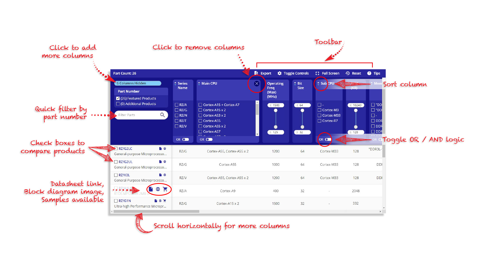
Tips for Using This Parametric Table:
- Hide Filters button in header: Collapse or expands filters
- Column sort buttons in header: Sort Column alphabetically / numerically descending or ascending
- Reset button in header: Reset all filters to the page default
- Full Screen button in header: Expand the table to full screen view (user must close out of full screen before they can interact with rest of page)
- Export button in header: Export the filtered results of the table to an Excel document
- Filter parts search bar in header: Type to filter table results by part number
- Hide column button in column headers: Select to hide columns in table
- AND / OR toggle switches in header: Toggles the logic of this particular filter to be “AND” or “OR” logic for filtering results
- Multiselect checkboxes at beginning of each row in table: Select these checkboxes to compare products against each other
- Document icon next to product name in row: View the featured document for this product
- Chip icon next to the right of the document icon in row: View the block diagram for this product
- Cart icon to the right of the chip icon: Indicates that samples are available for this product