
PCI Express® Jitter Attenuator
以下のデバイスを代替品として推奨しております。
ページセクションへ移動:
概要
説明
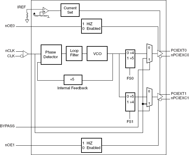
The 9DB202 is a high performance 1-to-2 Differential-to-HCSL Jitter Attenuator designed for use in PCI Express®™ systems. In some PCI Express®™ systems, such as those found in desktop PCs, the PCI Express®™ clocks are generated from a low bandwidth, high phase noise PLL frequency synthesizer. In these systems, a jitter-attenuating device may be necessary in order to reduce high frequency random and deterministic jitter components from the PLL synthesizer and from the system board. The 9DB202 has two PLL bandwidth modes. In low bandwidth mode, the PLL loop bandwidth is 500kHz. This setting offers the best jitter attenuation and is still high enough to pass a triangular input spread spectrum profile. In high bandwidth mode, the PLL bandwidth is at 1MHz and allows the PLL to pass more spread spectrum modulation. For serdes which have x10 reference multipliers instead of x12.5 multipliers, each of the two PCI Express®™ outputs (PCIEX0:1) can be set for 125MHz instead of 100MHz by configuring the appropriate frequency select pins (FS0:1).
特長
- Two 0.7V current mode differential HCSL output pairs
- One differential clock input
- CLK and nCLK supports the following input types: LVPECL, LVDS, LVHSTL, SSTL, HCSL
- Maximum output frequency: 140MHz
- Input frequency range: 90MHz - 140MHz
- VCO range: 450MHz - 700MHz
- Output skew: 110ps (maximum)
- Cycle-to-cycle jitter: 110ps (maximum)
- RMS phase jitter @ 100MHz, (1.5MHz - 22MHz): 2.42ps (typical)
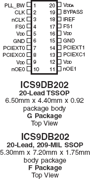
- 3.3V operating supply
- 0°C to 70°C ambient operating temperature
- Available in lead-free RoHS compliant package
- Industrial temperature information available upon request
製品比較
アプリケーション
設計・開発
モデル
ECADモデル
[製品選択]テーブル内の製品名をクリックするとSamacSysが提供する回路図シンボル、PCBフットプリント、3D CADモデルがご確認いただけます。 お探しのシンボルやモデルが見つからない場合、Webサイトから直接リクエストできます。

Processing table
| SSOP | 20 | C | Yes | Tube | ||
| SSOP | 20 | C | Yes | Reel | ||
| TSSOP | 20 | C | Yes | Tube | ||
| TSSOP | 20 | C | Yes | Reel |

Tips for Using This Parametric Table:
- Hide Filters button in header: Collapse or expands filters
- Column sort buttons in header: Sort Column alphabetically / numerically descending or ascending
- Reset button in header: Reset all filters to the page default
- Full Screen button in header: Expand the table to full screen view (user must close out of full screen before they can interact with rest of page)
- Export button in header: Export the filtered results of the table to an Excel document
- Filter parts search bar in header: Type to filter table results by part number
- Hide column button in column headers: Select to hide columns in table
- AND / OR toggle switches in header: Toggles the logic of this particular filter to be “AND” or “OR” logic for filtering results
- Multiselect checkboxes at beginning of each row in table: Select these checkboxes to compare products against each other
- Document icon next to product name in row: View the featured document for this product
- Chip icon next to the right of the document icon in row: View the block diagram for this product
- Cart icon to the right of the chip icon: Indicates that samples are available for this product
ビデオ&トレーニング
PCIe Clocking Architectures (Common and Separate)

Video List