
LVPECL FemtoClock Dynamic Clock Switch/Generator
NOTICE - The following device(s) are recommended alternatives:
Jump to Page Section:
Overview
Description
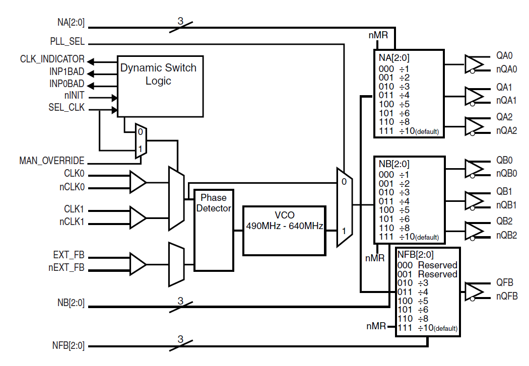
The 873995 is a Zero Delay/Multiplier/Divider with hitless input clock switching capability. The 873995 is ideal for use in redundant, fault tolerant clock trees where low phase noise and low jitter are critical. The device receives two differential LVPECL clock signals from which it generates 6 LVPECL clock outputs with "zero" delay. The output divider and feedback divider selections also allow for frequency multiplication or division. The 873995 Dynamic Clock Switch (DCS) circuit continuously monitors both input clock signals. Upon detection of a failure (input clock stuck LOW or HIGH for at least 1 period), INP_BAD for that clock will be set HIGH. If that clock is the primary clock, the DCS will switch to the good secondary clock and phase/frequency alignment will occur with minimal output phase disturbance. The low jitter characteristics combined with input clock monitoring and automatic switching from bad to good input clocks make the 873995 an ideal choice for mission critical applications that utilize 1G or 10G Ethernet or 1G/4G/10G Fibre Channel.
Features
- Six differential 3.3V LVPECL outputs
- Selectable differential clock inputs
- CLKx, nCLKx pair can accept the following differential input levels: LVPECL, LVDS, LVHSTL, HCSL, SSTL
- Input clock frequency range: 49MHz to 213.33MHz
- Output clock frequency range: 49MHz to 640MHz
- VCO range: 490MHz to 640MHz
- External feedback for "zero delay" clock regeneration with configurable frequencies
- Output skew: 100ps (maximum)
- RMS phase jitter (1.875MHz - 20MHz): 0.77ps (typical) assuming a low phase noise reference clock input
- 3.3V supply voltage
- 0°C to 70°C ambient operating temperature
- Available in lead-free (RoHS 6) package
Comparison
Applications
Design & Development
Models
ECAD Models
Schematic symbols, PCB footprints, and 3D CAD models from SamacSys can be found by clicking on products in the Product Options table. If a symbol or model isn't available, it can be requested directly from the website.

Processing table
| PTQFP | 48 | C | Yes | Tray | ||
| PTQFP | 48 | C | Yes | Reel |

Tips for Using This Parametric Table:
- Hide Filters button in header: Collapse or expands filters
- Column sort buttons in header: Sort Column alphabetically / numerically descending or ascending
- Reset button in header: Reset all filters to the page default
- Full Screen button in header: Expand the table to full screen view (user must close out of full screen before they can interact with rest of page)
- Export button in header: Export the filtered results of the table to an Excel document
- Filter parts search bar in header: Type to filter table results by part number
- Hide column button in column headers: Select to hide columns in table
- AND / OR toggle switches in header: Toggles the logic of this particular filter to be “AND” or “OR” logic for filtering results
- Multiselect checkboxes at beginning of each row in table: Select these checkboxes to compare products against each other
- Document icon next to product name in row: View the featured document for this product
- Chip icon next to the right of the document icon in row: View the block diagram for this product
- Cart icon to the right of the chip icon: Indicates that samples are available for this product