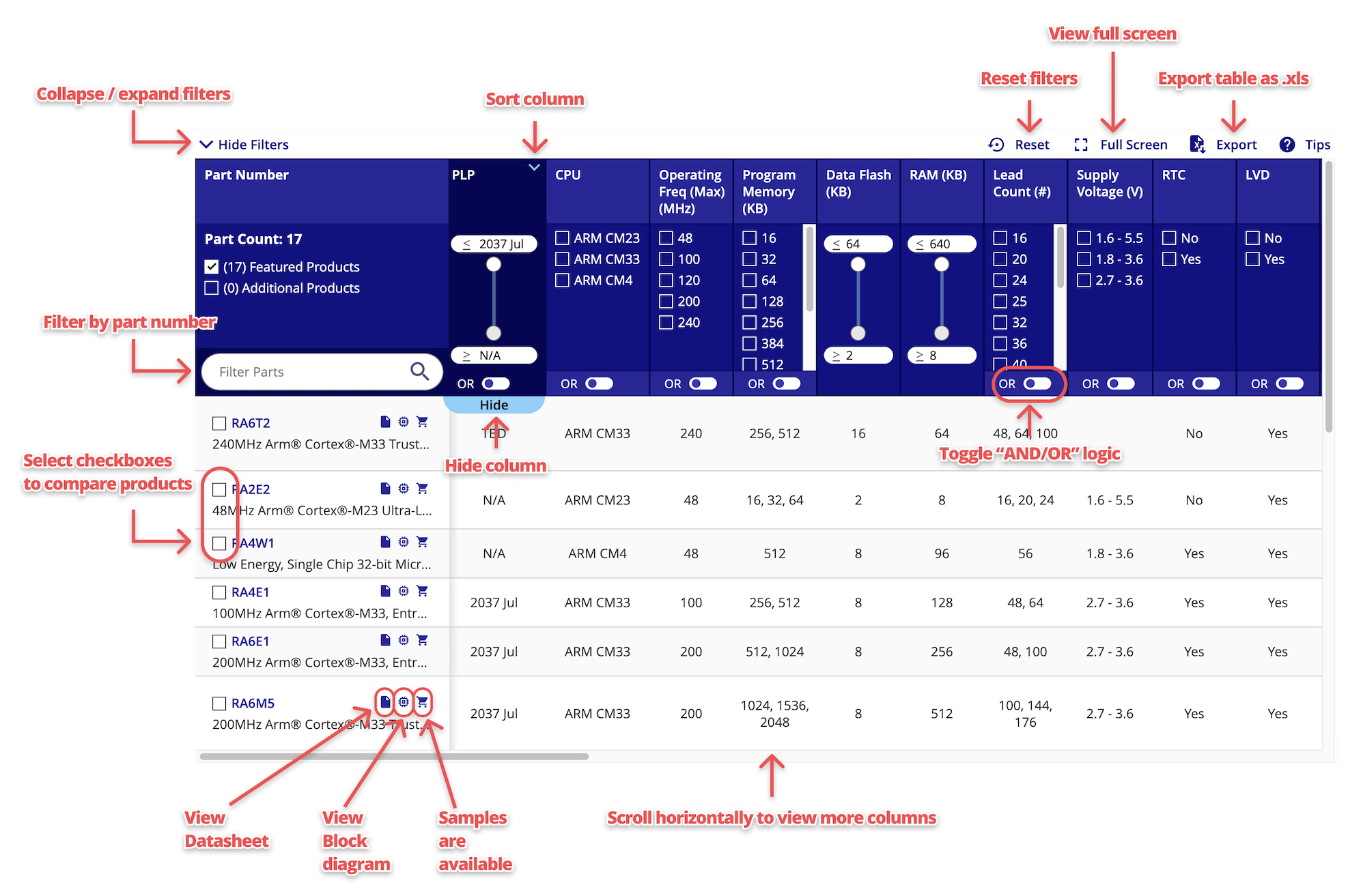
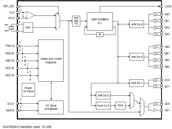
Image


Renesas clock generators and synthesizers generate one or more clock signals from crystals and/or clean input sources, such as those from crystal oscillators (XOs). If the input reference has more noise than can be tolerated on the outputs, visit the jitter attenuators page for more information. This extreme performance category contains clock generators suitable for providing reference clocks to PHY and switch modules supporting serial data applications up to 400Gbps and beyond.
Many of these devices support multiple different output frequencies. The use of integer and fractional PLL technologies and integer or fractional output divider technologies allow many of these devices to generate outputs that are unrelated to input frequencies, or in some cases, unrelated to other output frequencies. Most devices also provide options for output frequencies that are integer ratios of one another and track the same input. If more than one unique output frequency is required (e.g., 100MHz and 125MHz), use the Output Banks filter in the parametric table. Each bank corresponds to a unique output frequency. The number of outputs per bank is highly variable depending on the clock generator.
Once the clock generator is selected, fanout buffers can be used to provide additional copies and types (LVCMOS, LVPECL, etc.) of outputs. Renesas has the largest selection of timing products in the industry, which allows for highly optimized full clock tree solutions.
Outputs (#) |
Output Type |
Output Freq Range (MHz) |
Input Freq (MHz) |
Inputs (#) |
Input Type |
Output Banks (#) |
Core Voltage (V) |
Output Voltage (V) |
Phase Jitter Typ RMS (ps) |
105°C Max. Case Temp. |
|
|---|---|---|---|---|---|---|---|---|---|---|---|
| Part Number | |||||||||||
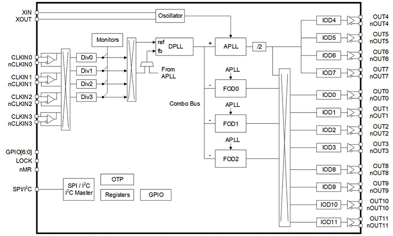
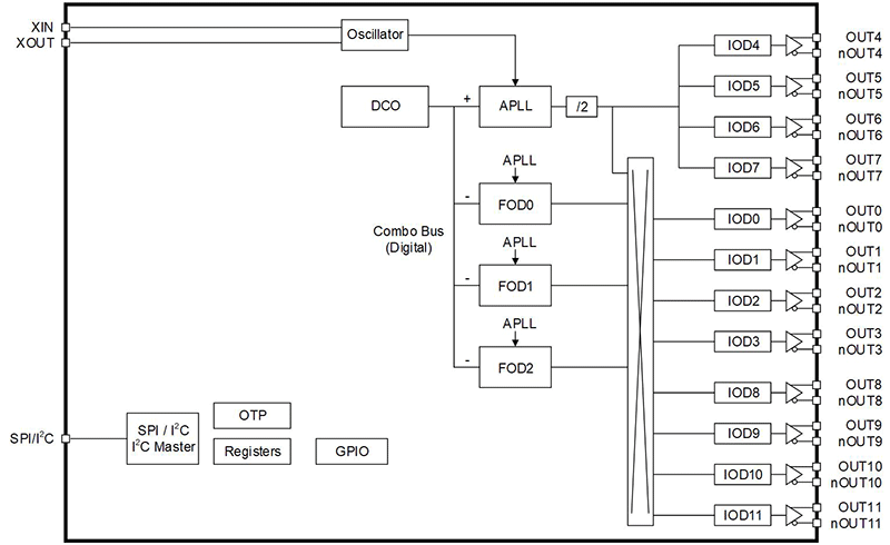
| FemtoClock™ 3 Ultra-Low Noise Jitter Attenuator and Multi-Frequency Clock Synthesizer | 8, 16 | LP-HCSL, LVCMOS, LVDS | 0.001 - 650 | 1 - 650 | 3 | Crystal, LP-HCSL, LVCMOS, LVDS | 6, 8, 12 | 1.8, 2.5, 3.3 | 1.8, 2.5, 3.3 | 0.15 | |
| FemtoClock™ 3 Ultra-Low Noise Multi-Frequency Clock Synthesizer | 8, 12 | LP-HCSL, LVCMOS, LVDS | 0.001 - 650 | 1 - 650 | 4 | Crystal, LP-HCSL, LVCMOS, LVDS | 6 | 1.8, 2.5, 3.3 | 1.8, 2.5, 3.3 | 0.15 | |
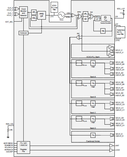
| JESD204B/C Clock Jitter Attenuator | 12 | LVDS, LVPECL | 15.625 - 2500 | 0.008 - 250 | 2 | LVDS, LVPECL | 5 | 3.3 | 3.3 | 0.075 | |
| FemtoClock™ NG 12-Output Clock Generator | 12 | HCSL | 10.91 - 2500 | 5 - 1000 | 2 | Crystal, HCSL, HSTL, LVCMOS, LVDS, LVHSTL, LVPECL | 4 | 3.3 | 3.3 | 0.095 | |
| FemtoClock™ NG 12-Output Clock Generator | 12 | LVDS, LVPECL | 10.91 - 2500 | 5 - 1000 | 2 | Crystal, HCSL, HSTL, LVCMOS, LVDS, LVHSTL, LVPECL | 4 | 3.3 | 3.3 | 0.089 | |
| FemtoClock™ NG 12-Output Clock Generator | 12 | LVDS, LVPECL | 10.91 - 2500 | 5 - 1000 | 2 | Crystal, HCSL, HSTL, LVCMOS, LVDS, LVHSTL, LVPECL | 4 | 3.3 | 3.3 | 0.08 | |
| FemtoClock™ 2 Clock Generator | 4 | HCSL, LVCMOS, LVDS | 10 - 1000 | 25 - 312.5 | 2 | Crystal, HCSL, LVCMOS, LVDS | 4 | 1.8, 3.3 | 1.8 | 0.079 | |
| FemtoClock™ 2 Clock Generator | 4 | HCSL, LVCMOS, LVDS | 10 - 1000 | 0 | 4 | 1.8, 3.3 | 1.8 | 0.079 | |||
| FemtoClock™ 2 Jitter Attenuator or Clock Generator | 4 | HCSL, LVCMOS, LVDS | 10 - 1000 | 5 - 1000 | 3 | Crystal, HCSL, LVCMOS, LVDS | 4 | 1.8, 3.3 | 1.8 | 0.079 | |
| FemtoClock 2 Jitter Attenuator or Clock Generator | 8 | HCSL, LVCMOS, LVDS | 10 - 1000 | 1 - 800 | 3 | Crystal, HCSL, LVCMOS, LVDS | 8 | 1.8, 3.3 | 1.8 | 0.067 | No |
| FemtoClock™ 2 Jitter Attenuator or Clock Generator | 4 | HCSL, LVCMOS, LVDS | 10 - 1000 | 1 - 800 | 3 | Crystal, HCSL, LVCMOS, LVDS | 4 | 1.8, 3.3 | 1.8 | 0.079 |