
概要
説明
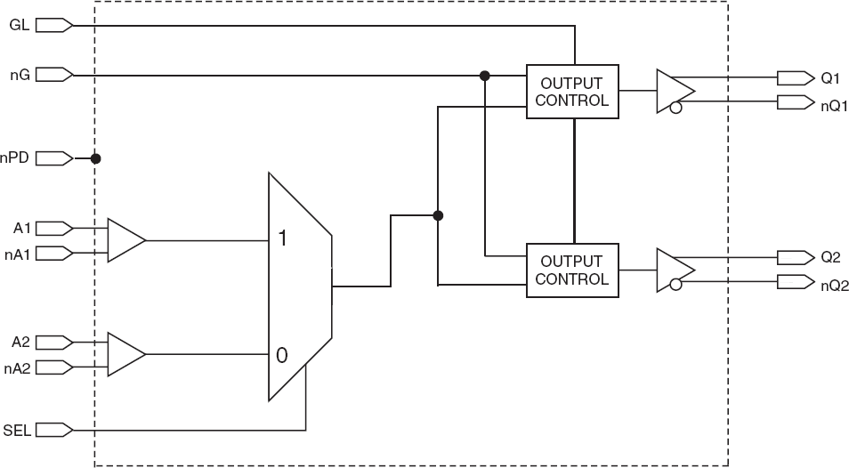
The 5T9302I 2.5V differential clock buffer is a user-selectable differential input to two LVDS outputs. The fanout from a differential input to two LVDS outputs reduces loading on the preceding driver and provides an efficient clock distribution network. The 5T9302I can act as a translator from a differential HSTL, eHSTL, LVEPECL (2.5V), LVPECL (3.3V), CML, or LVDS input to LVDS outputs. A single-ended 3.3V / 2.5V LVTTL input can also be used to translate to LVDS outputs. The redundant input capability allows for an asynchronous change-over from a primary clock source to a secondary clock source. Selectable reference inputs are controlled by SEL. The 5T9302I outputs can be asynchronously enabled/ disabled. When disabled, the outputs will drive to the value selected by the GL pin. Multiple power and grounds reduce noise.
特長
- Guaranteed low skew: 50ps (maximum)
- Very low duty cycle distortion: 125ps (maximum)
- High speed propagation delay: 1.5ns (maximum)
- Up to 450MHz operation
- Selectable inputs
- Hot insertable and over-voltage tolerant inputs
- 3.3V/2.5V LVTTL, HSTL eHSTL, LVEPECL (2.5V), LVPECL (3.3V), CML or LVDS input interface
- Selectable differential inputs to two LVDS outputs
- Power-down mode
- 2.5V VDD
- -40°C to 85°C ambient operating temperature
- Available in Lead-free (RoHS 6) package
製品比較
アプリケーション
設計・開発
モデル
ECADモデル
[製品選択]テーブル内の製品名をクリックするとSamacSysが提供する回路図シンボル、PCBフットプリント、3D CADモデルがご確認いただけます。 お探しのシンボルやモデルが見つからない場合、Webサイトから直接リクエストできます。

Processing table
| TSSOP | 20 | I | Yes | Tube | ||
| TSSOP | 20 | I | Yes | Reel |

Tips for Using This Parametric Table:
- Hide Filters button in header: Collapse or expands filters
- Column sort buttons in header: Sort Column alphabetically / numerically descending or ascending
- Reset button in header: Reset all filters to the page default
- Full Screen button in header: Expand the table to full screen view (user must close out of full screen before they can interact with rest of page)
- Export button in header: Export the filtered results of the table to an Excel document
- Filter parts search bar in header: Type to filter table results by part number
- Hide column button in column headers: Select to hide columns in table
- AND / OR toggle switches in header: Toggles the logic of this particular filter to be “AND” or “OR” logic for filtering results
- Multiselect checkboxes at beginning of each row in table: Select these checkboxes to compare products against each other
- Document icon next to product name in row: View the featured document for this product
- Chip icon next to the right of the document icon in row: View the block diagram for this product
- Cart icon to the right of the chip icon: Indicates that samples are available for this product