

| CAD Model: | View CAD Model |
| Pkg. Type: | VFQFPN |
| Pkg. Code: | NLG72 |
| Lead Count (#): | 72 |
| Pkg. Dimensions (mm): | 10.0 x 10.0 x 1.0 |
| Pitch (mm): | 0.5 |
| Moisture Sensitivity Level (MSL) | 3 |
| Pb (Lead) Free | Yes |
| ECCN (US) | EAR99 |
| HTS (US) | 8542.39.0090 |
| Lead Count (#) | 72 |
| Carrier Type | Tray |
| Moisture Sensitivity Level (MSL) | 3 |
| Qty. per Reel (#) | 0 |
| Qty. per Carrier (#) | 168 |
| Pb (Lead) Free | Yes |
| Pb Free Category | e3 Sn |
| Temp. Range (°C) | -40 to 85°C |
| 105°C Max. Case Temp. | 0 |
| Adjustable Phase | Yes |
| Advanced Features | PWM Encoder/Decoder, ToD, 1PPS, DCO, IEEE 1588, JESD204B, JESD204C, T-BC, T-TSC Class C, eEEC |
| Application | Wireless Baseband Unit (BBU), Distributed Unit (DU), Centralized Unit (CU), Radio Unit (RU) |
| Channels (#) | 6 |
| Core Voltage (V) | 2.5V, 3.3V |
| DPLL Channels (#) | 6 |
| Diff. Inputs | 5 |
| Diff. Outputs | 12 |
| Family Name | ClockMatrix |
| Feedback Divider Resolution (bits) | 48 |
| Fractional Output Dividers (#) | 6 |
| Input Freq (MHz) | 0.001 - 1000 |
| Input Redundancy | Input Monitor, Digital holdover, Hitless switch, Phase-slope limiting |
| Input Ref. Divider Resolution (bits) | 4 |
| Input Type | HCSL, LVDS, LVHSTL, LVPECL, SSTL |
| Inputs (#) | 10 |
| JESD204B/C Compliant | Yes |
| Length (mm) | 10 |
| Longevity | 2040 Apr |
| Loop Bandwidth Range (Hz) | 0.0001 - 12000 |
| MOQ | 168 |
| Noise Floor (dBc/Hz) | -158 |
| Output Banks (#) | 6 |
| Output Divider Resolution (bits) | 32 |
| Output Freq Range (MHz) | 5.0E-7 - 1000 |
| Output Skew (ps) | 50 |
| Output Type | HSTL, LVCMOS, LVDS, LVHSTL, LVPECL, LVTTL |
| Output Voltage (V) | 1.2V, 1.5V, 1.8V, 2.5V, 3.3V |
| Outputs (#) | 24 |
| Phase Jitter Typ RMS (ps) | 0.15 |
| Phase Noise Supports GSM | No |
| Pitch (mm) | 0.5 |
| Pkg. Dimensions (mm) | 10.0 x 10.0 x 1.0 |
| Pkg. Type | VFQFPN |
| Product Category | FemtoClock NG |
| Prog. Interface | I2C, SPI |
| Published | No |
| Reference Output | No |
| Requires Terms and Conditions | Requires acceptance of Terms and Conditions |
| Spread Spectrum | No |
| Supply Voltage (V) | 3.3 - 3.3, 2.5 - 2.5, 1.8 - 1.8 |
| Synthesis Mode | Fractional, Integer |
| Tape & Reel | No |
| Thickness (mm) | 1 |
| Width (mm) | 10 |
| Xtal Freq (KHz) | 25 - 54 |
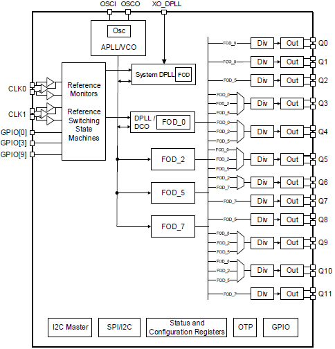
The RC32012A regenerates and distributes ultra-low jitter clock outputs and features up to four independent frequency domains that can be either locked to the external reference clock or locked to a free-run crystal or oscillator. Digital PLLs (DPLLs) support hitless reference switching between references from redundant timing sources. The device supports multiple independent timing channels for IEEE 1588 clock synthesis, SyncE clock generation, jitter attenuation, and radio clock generation including SYSREF generation for converters. Input-to-input, input-to-output and output-to-output phase skew can all be precisely managed. The device outputs ultra-low jitter clocks that can directly synchronize SerDes running at up to 56Gbps; as well as CPRI/OBSAI, SONET/SDH ADC/DAC. The RC32012A is ideal for use in 100G/200G/400G/800G telecom switch line cards, fabric cards, and wireless small cell applications.
To see other devices in this product family, visit the ClockMatrix™ Timing Solutions page.