

| CAD Model: | View CAD Model |
| Pkg. Type: | VFQFPN |
| Pkg. Code: | NXG28 |
| Lead Count (#): | 28 |
| Pkg. Dimensions (mm): | 4.0 x 4.0 x 1.5 |
| Pitch (mm): | 0.4 |
| Moisture Sensitivity Level (MSL) | 3 |
| Pb (Lead) Free | Yes |
| ECCN (US) | EAR99 |
| HTS (US) | 8542.39.0090 |
| Lead Count (#) | 28 |
| Carrier Type | Tray |
| Moisture Sensitivity Level (MSL) | 3 |
| Qty. per Reel (#) | 0 |
| Qty. per Carrier (#) | 490 |
| Pb (Lead) Free | Yes |
| Pb Free Category | e3 Sn |
| Temp. Range (°C) | -40 to 85°C |
| Assembly Location | MALAYSIA |
| Wafer Fab Location | SINGAPORE |
| Advanced Features | 4-Output Clock Generator |
| Application | Clock Generator |
| Channels (#) | 1 |
| Core Voltage (V) | 1.8V, 3.3V |
| Diff. Inputs | 0 |
| Diff. Outputs | 4 |
| Family Name | FemtoClock Clock Generator |
| Feedback Divider | 1 - 255 |
| Feedback Input | No |
| Fractional Output Dividers (#) | 1 |
| Inputs (#) | 0 |
| Length (mm) | 4 |
| Longevity | 2040 Apr |
| MOQ | 490 |
| Output Banks (#) | 4 |
| Output Freq Range (MHz) | 10 - 1000 |
| Output Signaling | LVPECL, LVDS |
| Output Skew (ps) | 50 |
| Output Type | LVCMOS, HCSL, LVDS |
| Output Voltage (V) | 1.8V |
| Outputs (#) | 4 |
| Package Area (mm²) | 81 |
| Phase Jitter Max RMS (ps) | 0.1 |
| Phase Jitter Typ RMS (fs) | 79 |
| Phase Jitter Typ RMS (ps) | 0.079 |
| Pitch (mm) | 0.4 |
| Pkg. Dimensions (mm) | 4.0 x 4.0 x 1.5 |
| Pkg. Type | VFQFPN |
| Product Category | FemtoClock 2, Ultra-Low Jitter Clocks (<300 fs RMS), Extreme Performance Clocks (<150 fs RMS), Network Synchronization, PDH and SONET/SDH Clocks, Programmable Clocks |
| Prog. Clock | Yes |
| Prog. Interface | I2C, SPI |
| Reference Output | No |
| Requires Terms and Conditions | Does not require acceptance of Terms and Conditions |
| Spread Spectrum | No |
| Tape & Reel | No |
| Thickness (mm) | 1.5 |
| VCO Max Freq (MHz) | 10700 |
| VCO Min Freq (MHz) | 9700 |
| Width (mm) | 4 |
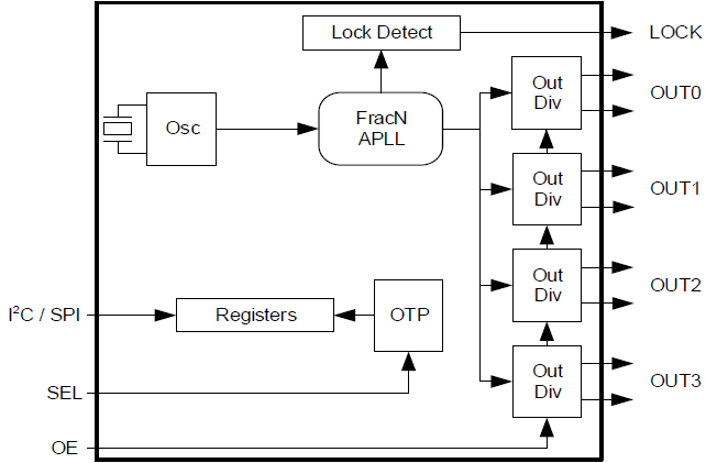
The RC22514A is a small, low-power timing component designed to be placed immediately adjacent to a PHY, switch, ASIC or FPGA that requires several reference clocks with jitter performance less than 100fs (max). The RC22514A can act as a frequency synthesizer to locally generate the reference clock or as a DCO for frequency margining or OTN clock applications, relying on an internal crystal reference source.