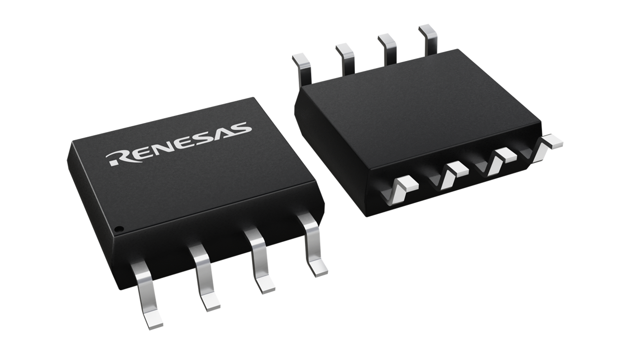

Package Information
| CAD Model: | View CAD Model |
| Pkg. Type: | SOIC |
| Pkg. Code: | DCG8 |
| Lead Count (#): | 8 |
| Pkg. Dimensions (mm): | 4.9 x 3.9 x 1.5 |
| Pitch (mm): | 1.27 |
Environmental & Export Classifications
| Pb (Lead) Free | Yes |
| Moisture Sensitivity Level (MSL) | 1 |
| ECCN (US) | |
| HTS (US) |
Product Attributes
| Pkg. Type | SOIC |
| Lead Count (#) | 8 |
| Pb (Lead) Free | Yes |
| Carrier Type | Tube |
| Accepts Spread Spec Input | No |
| Advanced Features | Reference Output |
| Core Voltage (V) | 3.3 |
| Feedback Input | No |
| Input Freq (MHz) | 13.5 - 13.5 |
| Input Type | Crystal, LVCMOS |
| Inputs (#) | 2 |
| Length (mm) | 4.9 |
| MOQ | 291 |
| Moisture Sensitivity Level (MSL) | 1 |
| Output Banks (#) | 1 |
| Output Freq Range (MHz) | 13.5 - 13.5, 27 - 27, 54 - 54 |
| Output Type | LVCMOS |
| Output Voltage (V) | 3.3 |
| Outputs (#) | 3 |
| Package Area (mm²) | 19.1 |
| Pb Free Category | e3 Sn |
| Period Jitter Typ P-P (ps) | 150 |
| Pitch (mm) | 1.27 |
| Pkg. Dimensions (mm) | 4.9 x 3.9 x 1.5 |
| Prog. Clock | No |
| Qty. per Carrier (#) | 97 |
| Qty. per Reel (#) | 0 |
| Reference Output | Yes |
| Requires Terms and Conditions | Does not require acceptance of Terms and Conditions |
| Spread Spectrum | No |
| Supply Voltage (V) | 3.3 - 3.3 |
| Tape & Reel | No |
| Temp. Range (°C) | 0 to 70°C |
| Thickness (mm) | 1.5 |
| Width (mm) | 3.9 |
| Xtal Freq (KHz) | 13.5 - 13.5 |
| Xtal Inputs (#) | 1 |
Resources for MK3720
Description
The MK3720D is a drop-in replacement for the MK3720S and MK3720A devices. Compared to these earlier devices, the MK3720D offers a wider operating frequency range and improved power supply noise rejection. The MK3720 is a low cost, low jitter, high-performance 3.3 volt VCXO and PLL clock synthesizer designed to replace expensive 13.5, 27, or 54 MHz VCXOs. The patented on-chip Voltage Controlled Crystal Oscillator accepts a 0 to 3.3 V input voltage to cause the output clocks to vary by ±100 ppm. Using our patented VCXO and analog Phase-Locked Loop (PLL) techniques, the device uses an inexpensive external 13.5 MHz pullable crystal input to produce output clocks of 13.5 MHz, 27 MHz, and 54 MHz. The MK3720D exhibits a moderate VCXO gain of 120 ppm/V typical, when used with a high-quality external pullable quartz crystal. The frequency of the on-chip VCXO is adjusted by an external control voltage input into pin VIN. Because VIN is a high impedance input, it can be driven directly from a PWM RC integrator circuit.