| CAD Model: | View CAD Model |
| Pkg. Type: | TQFN |
| Pkg. Code: | L1D |
| Lead Count (#): | 12 |
| Pkg. Dimensions (mm): | 3.00 x 3.00 x 0.75 |
| Pitch (mm): | 0.5 |
| Moisture Sensitivity Level (MSL) | 3 |
| Pb (Lead) Free | Yes |
| ECCN (US) | EAR99 |
| HTS (US) | 8542.39.0090 |
| RoHS (ISL9120IRTAZ-T7A) | Download |
| Lead Count (#) | 12 |
| Carrier Type | Reel |
| Moisture Sensitivity Level (MSL) | 3 |
| Pitch (mm) | 0.5 |
| Pkg. Dimensions (mm) | 3.0 x 3.0 x 0.75 |
| Pb (Lead) Free | Yes |
| Pb Free Category | Pb-Free 100% Matte Tin Plate w/Anneal-e3 |
| Temp. Range (°C) | -40 to +85°C |
| Country of Assembly | MALAYSIA |
| Country of Wafer Fabrication | TAIWAN |
| Control Type | Hysteretic Mode |
| IQ [Rail 1] (µA) | 41 |
| Input Voltage (Max) (V) | 5.5 |
| Input Voltage (Max) [Rail 1] (V) | 5.5 - 5.5 |
| Input Voltage (Min) (V) | 1.8 |
| Input Voltage (Min) [Rail 1] (V) | 1.8 |
| Length (mm) | 3 |
| Longevity | 2033 Dec |
| MOQ | 250 |
| Output Current (Max) [Rail 1] (A) | 0.8 |
| Output Voltage (Max) (V) | 5.2 |
| Output Voltage (Max) [Rail 1] (V) | 5.2 |
| Output Voltage (Min) (V) | 1 |
| Output Voltage (Min) [Rail 1] (V) | 1 |
| Outputs (#) | 1 |
| POR | Yes |
| Parametric Category | Buck-boost Regulators (Integrated FETs) |
| Peak Efficiency (%) | 98 |
| Pkg. Type | TQFN |
| Price (USD) | $1.32835 |
| Qualification Level | Standard |
| Quiescent Current | 41 µA |
| SYNCH Capability | No |
| Thickness (mm) | 0.75 |
| Topology [Rail 1] | Buck-Boost |
| Width (mm) | 3 |
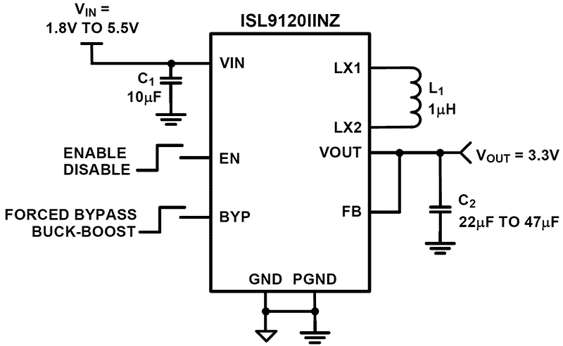
The ISL9120 and ISL9120IR are highly integrated buck-boost switching regulators that accept input voltages either above or below the regulated output voltage. The regulator automatically transitions between buck and boost modes without significant output disturbance. They also have automatic bypass functionality. When the input voltage is generally within 1% to 2% of the output voltage, there will be a direct bypass connection between the VIN and VOUT pins.
In addition to the automatic bypass functionality, the ISL9120 and ISL9120IR also have forced bypass functionality with the use of the BYP pin. The device is capable of delivering up to 800mA of output current (VIN = 2.5V, VOUT = 3.3V) and provides excellent efficiency due to its adaptive current limit Pulse Frequency Modulation (PFM) control architecture.
The ISL9120 and ISL9120IR are designed for stand-alone applications and support a 3.3V fixed output voltage or variable output voltages with an external resistor divider. The forced bypass power saving mode can be chosen if voltage regulation is not required. The device consumes less than 3.5µA of current over the operating temperature range in forced bypass mode.
The ISL9120 and ISL9120IR require only a single inductor and very few external components. Power supply solution size is minimized by the ISL9120 1.41mm x 1.41mm WLCSP package and the ISL9120IR 3mm x 3mm 12 Ld TQFN package.