
| CAD Model: | View CAD Model |
| Pkg. Type: | WLCSP-TKCURDLBC |
| Pkg. Code: | WEV |
| Lead Count (#): | 16 |
| Pkg. Dimensions (mm): | 1.78 x 1.78 x 0.54 |
| Pitch (mm): | 0.4 |
| Moisture Sensitivity Level (MSL) | 1 |
| Pb (Lead) Free | Yes |
| ECCN (US) | |
| HTS (US) |
| Lead Count (#) | 16 |
| Carrier Type | Reel |
| Moisture Sensitivity Level (MSL) | 1 |
| Pb (Lead) Free | Yes |
| Pb Free Category | Pb-Free Ball Terminal (SAC405)-e1 |
| Temp. Range (°C) | -40 to +85°C |
| Control Type | Current Mode |
| IQ [Rail 1] (µA) | 45 |
| Input Voltage (Max) (V) | 5.4 |
| Input Voltage (Max) [Rail 1] (V) | 5.4 - 5.4 |
| Input Voltage (Min) (V) | 2.35 |
| Input Voltage (Min) [Rail 1] (V) | 2.35 |
| Length (mm) | 1.8 |
| MOQ | 3000 |
| Output Current (Max) [Rail 1] (A) | 1.8 |
| Output Voltage (Max) (V) | 5.2 |
| Output Voltage (Max) [Rail 1] (V) | 5.2 |
| Output Voltage (Min) (V) | 3.15 |
| Output Voltage (Min) [Rail 1] (V) | 3.15 |
| Outputs (#) | 1 |
| POR | Yes |
| Parametric Category | Boost Regulators (Integrated FETs) |
| Peak Efficiency (%) | 96 |
| Pitch (mm) | 0.4 |
| Pkg. Dimensions (mm) | 1.8 x 1.8 x 0.54 |
| Pkg. Type | WLCSP-TKCURDLBC |
| Qualification Level | Standard |
| Quiescent Current | 45 µA |
| SYNCH Capability | No |
| Switching Frequency (KHz) | 2.9 - 2.9 |
| Switching Frequency Range (Typical) (kHz) | 2100 - 2900 |
| Thickness (mm) | 0.54 |
| Topology [Rail 1] | Boost |
| Width (mm) | 1.8 |
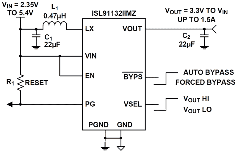
The ISL91132 is an integrated boost switching regulator for battery-powered applications. The device provides a power supply solution for products using a one-cell Li-ion or Li-polymer battery. The device is capable of delivering up to 1.8A output current from VIN = 2.5V and VOUT = 3.3V. The no-load quiescent current is only 108µA in Boost mode and 45µA in Forced Bypass mode, which significantly reduces the standby consumption.
The ISL91132 offers a Bypass mode operation where the output is directly connected to the input through a 38mΩ MOSFET to allow a significantly lower dropout voltage. The Bypass mode can be entered by an external command, or by auto bypass. The Forced Bypass mode allows the output voltage to operate close to the input voltage and improves the efficiency under these conditions.
The ISL91132 is designed to support six fixed output voltages ranging from 3.15V to 5V. A voltage select pin is available for each output variant to scale up the output voltage by a small offset to compensate for the load transient droop. The ISL91132 requires only an inductor and a few external components to operate. The 2.5MHz switching frequency further reduces the size of external components. The ISL91132 is available in a 16-bump, 0.4mm pitch, 1.78mm x 1.78mm WLCSP.