| Pitch (mm) | 1.27 |
| Lead Count (#) | 8 |
| Pkg. Dimensions (mm) | 4.9 x 3.9 x 1.5 |
| Pkg. Code | MSA |
| Pkg. Type | SOICN |
| Moisture Sensitivity Level (MSL) | 1 |
| Pb (Lead) Free | Yes |
| ECCN (US) | EAR99 |
| HTS (US) | 8542.39.0090 |
| RoHS (ICL7660CBAZ) | Download |
| Lead Count (#) | 8 |
| Carrier Type | Tube |
| Moisture Sensitivity Level (MSL) | 1 |
| Pitch (mm) | 1.3 |
| Pkg. Dimensions (mm) | 4.9 x 3.9 x 0.00 |
| Pb (Lead) Free | Yes |
| Pb Free Category | Pb-Free 100% Matte Tin Plate w/Anneal-e3 |
| Temp. Range | 0 to +70°C |
| Country of Assembly | China |
| Country of Wafer Fabrication | United States |
| Price (USD) | 1.29636 |
| IOUT (Max) (mA) | 20 |
| IS (Typical) | 170 µA |
| IS (mA) | 0.5 |
| Input Voltage (Max) (V) | 10 |
| Input Voltage (Min) (V) | 1.5 |
| Length (mm) | 4.9 |
| Longevity | 0000 Aug |
| MOQ | 3920 |
| Output Voltage (Max) (V) | -10 |
| Output Voltage (Min) (V) | -1.5 |
| Parametric Category | Charge Pumps (Inductorless) |
| Pkg. Type | SOICN |
| Qualification Level | Standard |
| Switching Frequency Range (Typical) (kHz) | 10 - 10 |
| Thickness (mm) | 0.00 |
| Width (mm) | 3.9 |
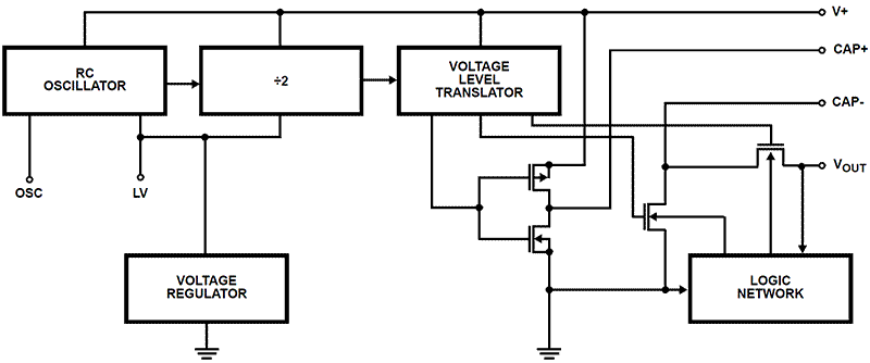
The Intersil ICL7660 and ICL7660A are monolithic CMOS power supply circuits which offer unique performance advantages over previously available devices. The ICL7660 performs supply voltage conversions from positive to negative for an input range of +1.5V to +10.0V resulting in complementary output voltages of -1.5V to -10.0V and the ICL7660A does the same conversions with an input range of +1.5V to +12.0V resulting in complementary output voltages of -1.5V to -12.0V. Only 2 noncritical external capacitors are needed for the charge pump and charge reservoir functions. The ICL7660 and ICL7660A can also be connected to function as voltage doublers and will generate output voltages up to +18.6V with a +10V input. Contained on the chip are a series DC supply regulator, RC oscillator, voltage level translator, and four output power MOS switches. A unique logic element senses the most negative voltage in the device and ensures that the output N-channel switch source-substrate junctions are not forward biased. This assures latchup free operation. The oscillator, when unloaded, oscillates at a nominal frequency of 10kHz for an input supply voltage of 5.0V. This frequency can be lowered by the addition of an external capacitor to the OSC terminal, or the oscillator may be overdriven by an external clock. The LV terminal may be tied to GROUND to bypass the internal series regulator and improve low voltage (LV) operation. At medium to high voltages (+3.5V to +10.0V for the ICL7660 and +3.5V to +12.0V for the ICL7660A), the LV pin is left floating to prevent device latchup.