
| CAD Model: | View CAD Model |
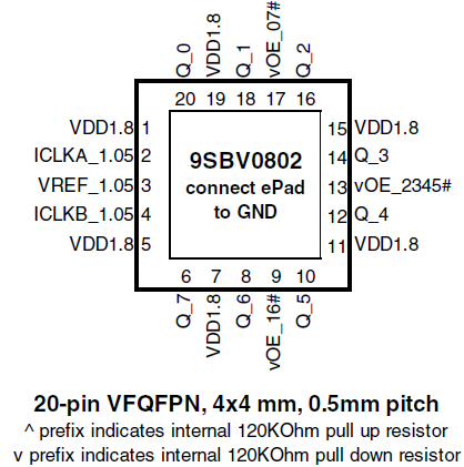
| Pkg. Type: | VFQFPN |
| Pkg. Code: | NLG20 |
| Lead Count (#): | 20 |
| Pkg. Dimensions (mm): | 4.0 x 4.0 x 1.0 |
| Pitch (mm): | 0.5 |
| Moisture Sensitivity Level (MSL) | 1 |
| Pb (Lead) Free | Yes |
| ECCN (US) | EAR99 |
| HTS (US) | 8542.39.0090 |
| Lead Count (#) | 20 |
| Carrier Type | Tray |
| Moisture Sensitivity Level (MSL) | 1 |
| Qty. per Reel (#) | 0 |
| Qty. per Carrier (#) | 490 |
| Pb (Lead) Free | Yes |
| Pb Free Category | e3 Sn |
| Temp. Range (°C) | -40 to 85°C |
| Assembly Location | TAIWAN |
| Wafer Fab Location | TAIWAN |
| Core Voltage (V) | 1.8 |
| Function | Buffer |
| Input Freq (MHz) | 200 |
| Input Type | LVCMOS |
| Inputs (#) | 1 |
| Length (mm) | 4 |
| MOQ | 490 |
| Output Banks (#) | 2 |
| Output Freq Range (MHz) | 1 - 48 |
| Output Signaling | LVCMOS |
| Output Skew (ps) | 50 |
| Output Type | LVCMOS |
| Output Voltage (V) | 1.8 |
| Outputs (#) | 8 |
| Package Area (mm²) | 9 |
| Pitch (mm) | 0.5 |
| Pkg. Dimensions (mm) | 4.0 x 4.0 x 1.0 |
| Pkg. Type | VFQFPN |
| Price (USD) | $7.5922 |
| Product Category | Clock Buffers & Drivers |
| Reference Output | Yes |
| Requires Terms and Conditions | Does not require acceptance of Terms and Conditions |
| Spread Spectrum | No |
| Tape & Reel | No |
| Thickness (mm) | 1 |
| Width (mm) | 4 |
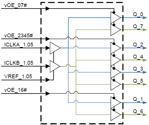
The 9SBV0802 provides two banks of four 1.05V LVCMOS outputs. Each bank has its own input. There are three OE pins. Two OE pins control two outputs each and one OE pin controls four outputs. One 9SBV0802 allows one PCH to easily support four CPUs with point-to-point routing of the PM signals. Two 9SBV0802 devices allow one PCH to easily support up to eight CPUs with point-to-point routing of the PM signals.