

| CAD Model: | View CAD Model |
| Pkg. Type: | VFQFPN |
| Pkg. Code: | NHG80 |
| Lead Count (#): | 80 |
| Pkg. Dimensions (mm): | 6.0 x 6.0 x 0.85 |
| Pitch (mm): | 0.5 |
| Moisture Sensitivity Level (MSL) | 3 |
| Pb (Lead) Free | Yes |
| ECCN (US) | EAR99 |
| HTS (US) | 8542.39.0090 |
| Lead Count (#) | 80 |
| Carrier Type | Tray |
| Moisture Sensitivity Level (MSL) | 3 |
| Qty. per Reel (#) | 0 |
| Qty. per Carrier (#) | 490 |
| Pb (Lead) Free | Yes |
| Pb Free Category | e4 NiPdAu |
| Temp. Range (°C) | -40 to 85°C |
| Assembly Location | TAIWAN, THAILAND |
| Wafer Fab Location | TAIWAN |
| Accepts Spread Spec Input | Yes |
| Additive Jitter | 7.4fs |
| Advanced Features | Multiple SMBus addresses, Side Band interface |
| App Jitter Compliance | 25G EDR, IF-UPI, PCIe Gen1, PCIe Gen2, PCIe Gen3, PCIe Gen4, PCIe Gen5, DB2000Q, QPI, UPI |
| Architecture | Common, SRIS, SRNS |
| C-C Jitter Max P-P (ps) | 50 |
| Chipset Manufacturer | Intel |
| Clock Spec. | DB2000QL |
| Core Voltage (V) | 3.3V |
| Diff. Input Signaling | HCSL |
| Diff. Inputs | 1 |
| Diff. Output Signaling | LP-HCSL |
| Diff. Outputs | 20 |
| Diff. Termination Resistors | 24 |
| Feedback Input | No |
| Function | Fanout Buffer |
| Input Freq (MHz) | 1 - 400 |
| Input Type | HCSL |
| Inputs (#) | 1 |
| Lead Compliant | No |
| Length (mm) | 6 |
| MOQ | 490 |
| Output Banks (#) | 1 |
| Output Enable (OE) Pins | 8 |
| Output Freq Range (MHz) | 1 - 400 |
| Output Impedance | 85 |
| Output Skew (ps) | 50 |
| Output Type | LP-HCSL |
| Output Voltage (V) | 0.7V |
| Outputs (#) | 20 |
| PLL | No |
| Package Area (mm²) | 81 |
| Pitch (mm) | 0.5 |
| Pkg. Dimensions (mm) | 6.0 x 6.0 x 0.85 |
| Pkg. Type | VFQFPN |
| Power Consumption Typ (mW) | 488 |
| Product Category | PCI Express Clocks, Processor Clock Buffers, Zero Delay Buffers |
| Reference Output | No |
| Spread Spectrum | Yes |
| Supply Voltage (V) | 3.3 - 3.3 |
| Tape & Reel | No |
| Thickness (mm) | 0.85 |
| Width (mm) | 6 |
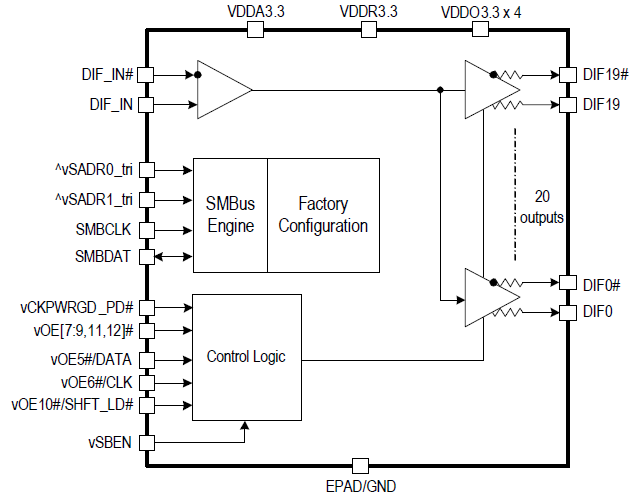
The 9QXL2001B is a 20-output very-low-additive phase jitter fanout buffer for PCIe Gen 4, Gen 5, and UPI applications. The 9QXL2001B provides two methods to control output enables; standard OE# pins and SMBus enable bits, or a simple 3-wire serial interface that is independent of the SMBus. The OE Control Mode is set via a hardware strap. It offers integrated terminations for 85Ω transmission lines.