Package Information
| CAD Model: | View CAD Model |
| Pkg. Type: | VFQFPN |
| Pkg. Code: | NDG40 |
| Lead Count (#): | 40 |
| Pkg. Dimensions (mm): | 5.0 x 5.0 x 0.9 |
| Pitch (mm): | 0.4 |
Environmental & Export Classifications
| Moisture Sensitivity Level (MSL) | 3 |
| Pb (Lead) Free | Yes |
| ECCN (US) | EAR99 |
| HTS (US) | 8542.39.0090 |
Product Attributes
| Lead Count (#) | 40 |
| Carrier Type | Tray |
| Moisture Sensitivity Level (MSL) | 3 |
| Qty. per Reel (#) | 0 |
| Qty. per Carrier (#) | 490 |
| Pb (Lead) Free | Yes |
| Pb Free Category | e3 Sn |
| Temp. Range (°C) | 0 to 70°C |
| Advanced Features | Spread Spectrum, Reference Output |
| App Jitter Compliance | PCIe Gen1, PCIe Gen2, PCIe Gen3 |
| Architecture | Common |
| C-C Jitter Max P-P (ps) | 50 |
| Core Voltage (V) | 1.5 |
| Diff. Output Signaling | LP-HCSL |
| Diff. Outputs | 6 |
| Diff. Termination Resistors | 12 |
| Function | Generator |
| Input Freq (MHz) | 25 - 25 |
| Input Type | Crystal, LVCMOS |
| Inputs (#) | 1 |
| Length (mm) | 5 |
| MOQ | 490 |
| Output Freq Range (MHz) | 25 - 25, 100 - 100 |
| Output Impedance | 33 |
| Output Skew (ps) | 50 |
| Output Type | LP-HCSL, LVCMOS |
| Output Voltage (V) | 0.8V, 1.5V |
| Outputs (#) | 7 |
| PLL | Yes |
| Package Area (mm²) | 25 |
| Pitch (mm) | 0.4 |
| Pkg. Dimensions (mm) | 5.0 x 5.0 x 0.9 |
| Pkg. Type | VFQFPN |
| Power Consumption Typ (mW) | 45 |
| Product Category | PCI Express Clocks |
| Prog. Clock | No |
| Reference Output | Yes |
| Requires Terms and Conditions | Does not require acceptance of Terms and Conditions |
| Spread Spectrum | Yes |
| Supply Voltage (V) | 1.5 - 1.5 |
| Tape & Reel | No |
| Thickness (mm) | 0.9 |
| Width (mm) | 5 |
| Xtal Freq (MHz) | 25 - 25 |
| Xtal Inputs (#) | 1 |
Resources for 9FGU0631
Description
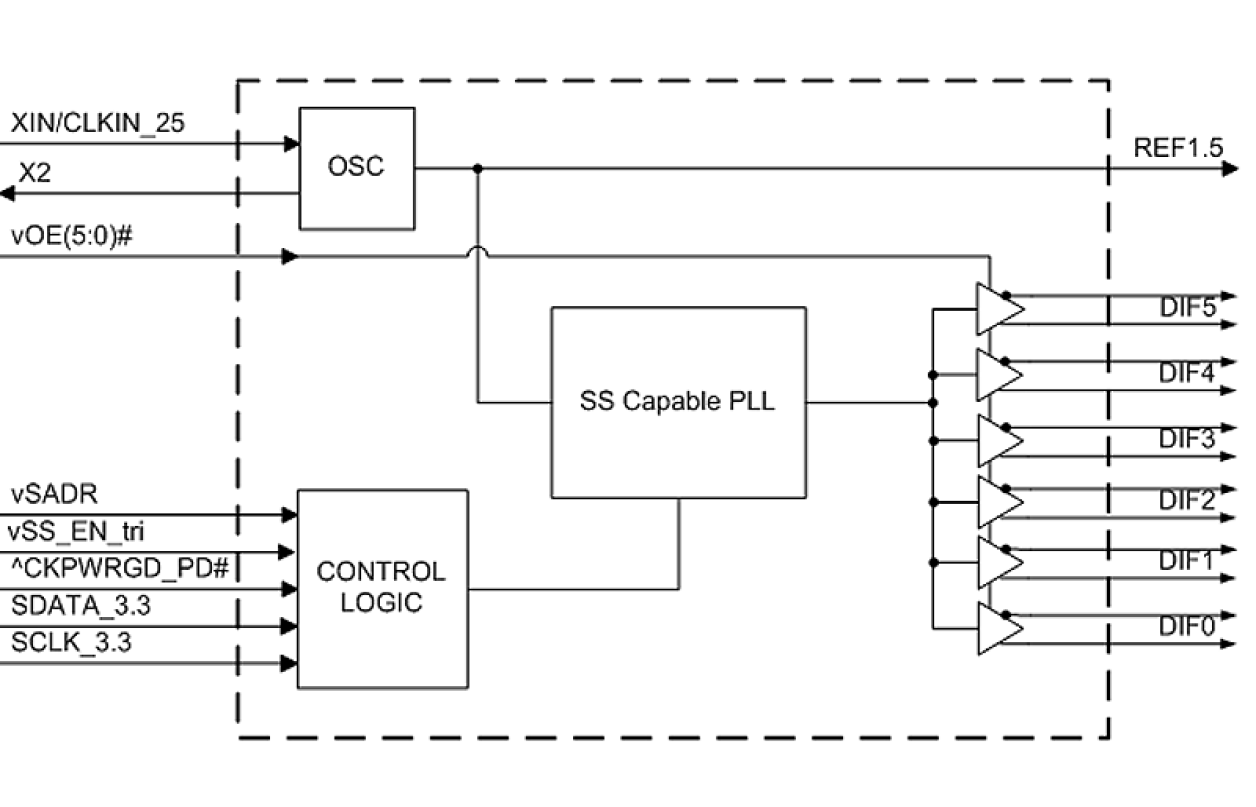
The 9FGU0631 is a member of IDT's 1.5 V Ultra-Low-Power PCIe clock family. The device has 6 output enables for clock management, 2 different spread spectrum levels in addition to spread off, and 2 selectable SMBus addresses.


