
| CAD Model: | View CAD Model |
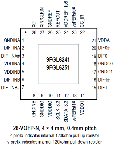
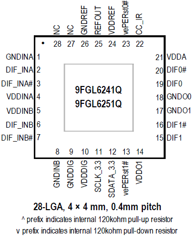
| Pkg. Type: | VFQFPN |
| Pkg. Code: | NDG28 |
| Lead Count (#): | 28 |
| Pkg. Dimensions (mm): | 4.0 x 4.0 x 0.9 |
| Pitch (mm): | 0.4 |
| Moisture Sensitivity Level (MSL) | 1 |
| Pb (Lead) Free | Yes |
| ECCN (US) | EAR99 |
| HTS (US) | 8542.39.0090 |
| Lead Count (#) | 28 |
| Carrier Type | Tray |
| Moisture Sensitivity Level (MSL) | 1 |
| Description | 33.33MHz external XTAL, SSC on (SRIS) |
| Advanced Features | Auto SRIS Mode |
| Input Freq (MHz) | 33.33 - 33.33 |
| Pkg. Dimensions (mm) | 4.0 x 4.0 x 0.9 |
| Qty. per Reel (#) | 0 |
| Qty. per Carrier (#) | 490 |
| Xtal Freq (MHz) | 33.33 - 33.33 |
| Pb (Lead) Free | Yes |
| Pb Free Category | e3 Sn |
| Temp. Range (°C) | -40 to 85°C |
| Country of Assembly | TAIWAN |
| Country of Wafer Fabrication | TAIWAN |
| App Jitter Compliance | PCIe Gen1, PCIe Gen2, PCIe Gen3, PCIe Gen4 |
| Architecture | Common, SRNS, SRIS |
| Diff. Input Signaling | HCSL, XTAL, LVCMOS |
| Diff. Inputs | 2 |
| Diff. Output Signaling | LP-HCSL |
| Diff. Outputs | 2 |
| Diff. Termination Resistors | 0 |
| Function | Zero Delay Buffer |
| Input Type | Crystal, LVCMOS |
| Inputs (#) | 1 |
| Length (mm) | 4 |
| MOQ | 490 |
| Output Banks (#) | 1 |
| Output Impedance | 100 |
| Output Type | LP-HCSL, LVCMOS |
| PLL | Yes |
| Package Area (mm²) | 25 |
| Pitch (mm) | 0.4 |
| Pkg. Type | VFQFPN |
| Power Consumption Typ (mW) | 65 |
| Price (USD) | $2.92708 |
| Prog. Clock | No |
| Published | No |
| Reference Output | Yes |
| Spread Spectrum | Yes |
| Supply Voltage (V) | 3.3 - 3.3 |
| Tape & Reel | No |
| Thickness (mm) | 0.9 |
| Width (mm) | 4 |
| Xtal Inputs (#) | 1 |
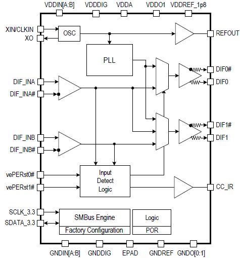
The 9FGL6241 is an intelligent buffer/clock generator tailored for single and dual-ported nVME SSDs. It supports Common (CC) and Independent Reference (IR) clocking architectures and is ideal for U.2 and M.2 form factors. The device is also useful in PCIe master/slave and clock multiplexing applications, with an internal clock generator as a third input channel.
For information regarding evaluation boards and material, please contact your local sales representative.